High electron energy based overlay error measurement methods and systems

a high electron energy and error measurement technology, applied in the direction of instruments, electrical appliances, material analysis, etc., can solve the problems of optical overlay measurement subject to various errors, misalignment or overlay error between each pair of layers, and complex integrated circuits that include multiple layers

Active Publication Date: 2012-11-22
APPL MATERIALS ISRAEL LTD
View PDF12 Cites 52 Cited by
  • Summary
  • Abstract
  • Description
  • Claims
  • Application Information

AI Technical Summary

Benefits of technology

[0030]According to an embodiment of the invention a system is provided and it may include: electron optics, arranged to: direct electrons of a primary electron beam to interact with a first area of a first layer of an inspected object: wherein the inspected object further may include a second layer that may include a second area; wherein the second layer is buried under the first layer: and direct high landing energy electrons of the primary electron beam to interact with the second area: at least one detector arranged to generate detection signals responsive to electrons that were scattered or reflected from at least one of the first and second areas; and a processor that may be arranged to determine at least one spatial relationship between at least one feature of the first area and at least one feature of the second area based on the detection signals, wherein an expected distance between a feature of the first area and a closest feature of the second layer is smaller than a pitch between adjacent features of the first area.

Problems solved by technology

Integrated circuits are very complex devices that include multiple layers.
Typically, the layers are misaligned. thus a misalignment or overlay error exists between each pair of layers.
Optical overlay measurements are subjected to various errors such as lens aberrations of the optical system.
It is noted that detecting overlay errors after the top layer is etched can be very costly.
This SEM has various disadvantages, such as not being capable of providing tilted images and is not efficient to provide images from holes of high aspect ratio.

Method used


Image

  • High electron energy based overlay error measurement methods and systems
  • High electron energy based overlay error measurement methods and systems
  • High electron energy based overlay error measurement methods and systems

Examples


Embodiment Construction

[0048]In the following detailed description, numerous specific details are set forth in order to provide a thorough understanding of the invention. However, it will be understood by those skilled in the art that the present invention may be practiced without these specific details. In other instances, well-known methods, procedures, and components have not been described in detail so as not to obscure the present invention.

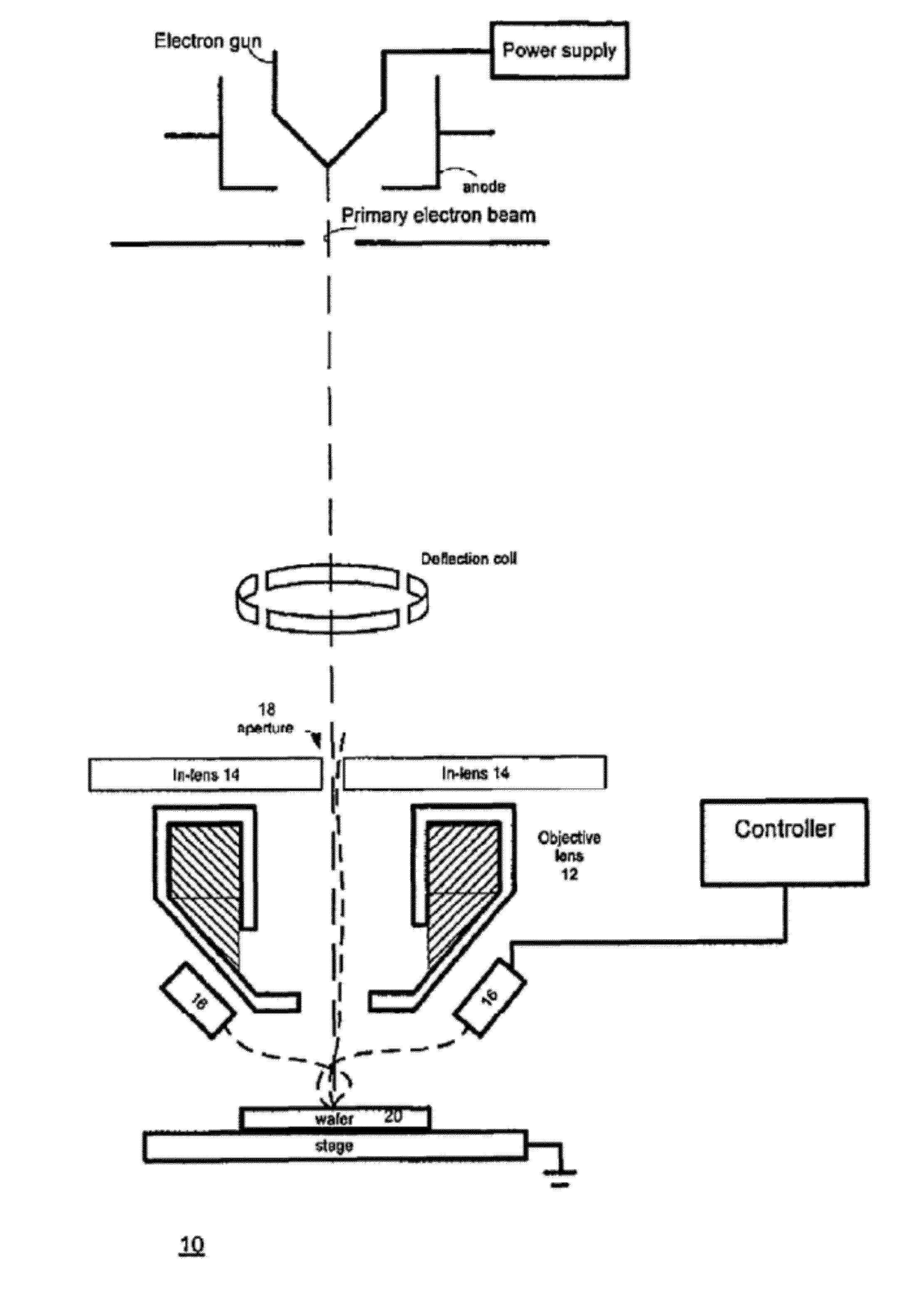
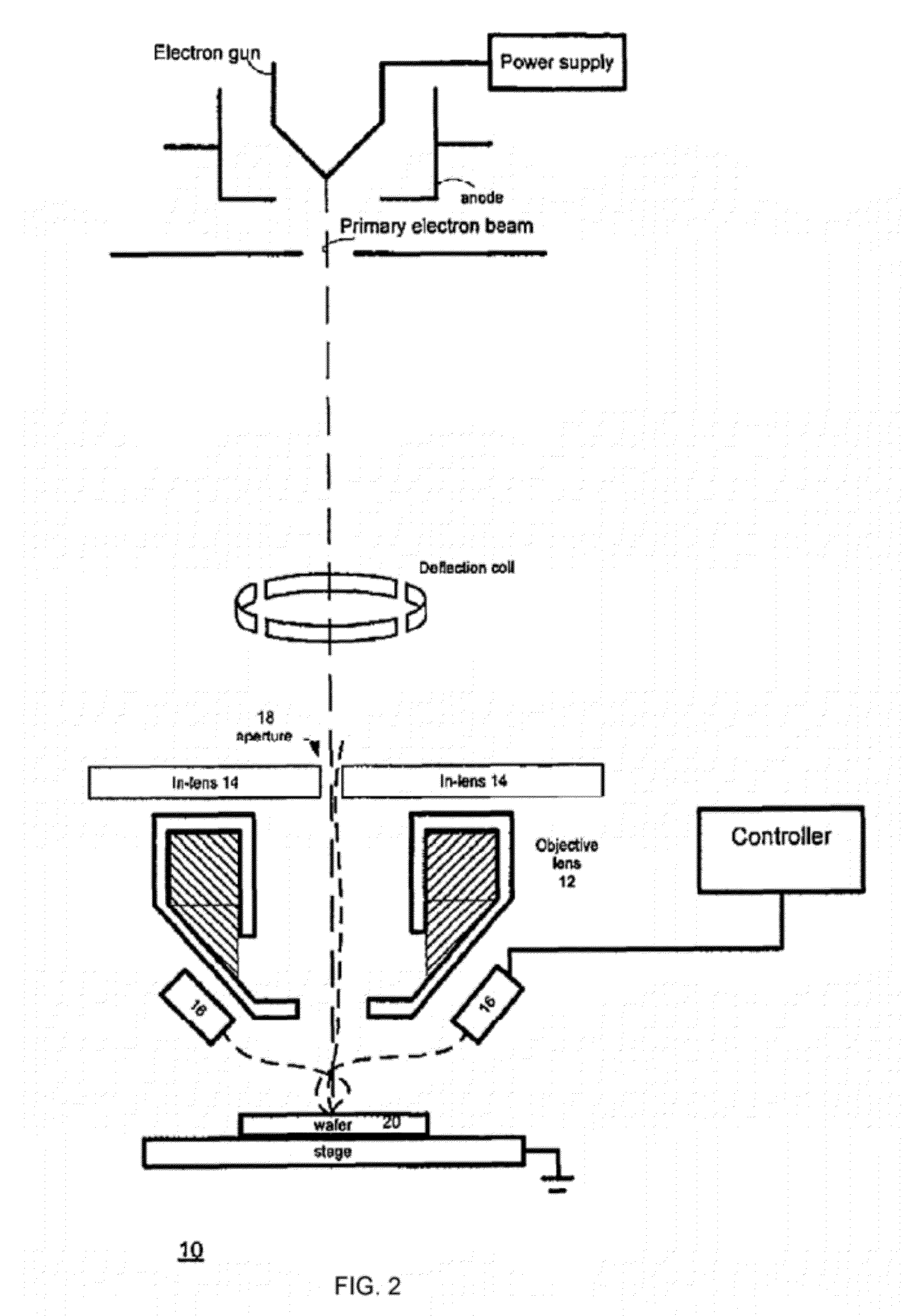
[0049]In all figures the same reference numbers represent the same elements.

[0050]According to various embodiments of the invention methods and systems for evaluating overlay errors are provided and include illuminating an inspected object with a primary electron beam that has electrons that have enough energy to interact with one or more buried layers. Secondary electrons and, additionally or alternatively, backscattered electrons are detected by in-lens and inner-lens detectors to provide detection signals. The detection signals are processed to provide an indic...


PUM

PropertyMeasurementUnit
areaaaaaaaaaaa
landing energyaaaaaaaaaa
distanceaaaaaaaaaa

Abstract

A method, a system and a computer readable medium are provided. The method may include obtaining or receiving first area information representative of a first area of a first layer of an inspected object; wherein the inspected object further comprises a second layer that comprises a second area; wherein the second layer is buried under the first layer; directing electrons of a primary electron beam to interact with the first area; directing electrons of the primary electron beam to interact with the second area; generating detection signals responsive to electrons that were scattered or reflected from at least one of the first and second areas; and determining at least one spatial relationship between at least one feature of the first area and at least one feature of the second area based on the detection signals and on the first area information.

Description

BACKGROUND OF THE INVENTIONOverlay Error Measurements[0001]Integrated circuits are very complex devices that include multiple layers. Each layer may include conductive material, isolating material while other layers may include semi-conductive materials. These various materials are arranged in patterns, usually in accordance with the expected functionality of the integrated circuit. The patterns also reflect the manufacturing process of the integrated circuits.[0002]Each layer is formed by a sequence of steps that usually includes depositing a resistive material on a substrate / layer, exposing the resistive material by a photolithographic process, and developing the exposed resistive material to produce a pattern that defines some areas to be later etched.[0003]Ideally, each layer is perfectly aligned to previously existing layer. Typically, the layers are misaligned. thus a misalignment or overlay error exists between each pair of layers.[0004]Various techniques evolved for observin...

Claims


Application Information

Patent Timeline
Patent Type & Authority Applications(United States)
IPC IPC(8): G01N23/20G01N23/00
CPCG01N23/2251G01N2223/611G01N2223/61G01B21/20H01J37/26
Inventor LANGER, MOSHEADAN, OFERPELTINOV, RAMUZIEL, YORAMSHOVAL, ORI
Owner APPL MATERIALS ISRAEL LTD
Why Eureka
Try Eureka