
Display panel and repair method thereof

Active Publication Date: 2012-11-29
TCL CHINA STAR OPTOELECTRONICS TECH CO LTD
View PDF3 Cites 30 Cited by
  • Summary
  • Abstract
  • Description
  • Claims
  • Application Information

AI Technical Summary

Benefits of technology

[0007]Therefore, an object of the present invention is to provide a flat display panel with a structure having repair lines and the method of repairing the broken lines thereof. After cell processes, laser is applied to cut and connect specific repair lines to bypass the breakings of the broken data line or scan line, so that signals which are unable to he transmitted through the broken data line or the broken scan line can be transmitted through the repair line. The flat display panel with a structure having repair lines and the method of repairing broken lines thereof can reduce scrapped products, thereby solving the problem occurring in the prior art.
[0013]In contrast to prior art, the present invention proposes a flat display panel with a structure having repair lines and the method of repairing the broken lines thereof. By using laser to cut any broken data line or scan line and then to connect specific repair lines, so that data signal or scan signal which is unable to be transmitted through the broken data line or the broken scan line can be transmitted through the repair lines. The flat display panel with a structure having repair lines and the method of repairing broken lines thereof can reduce scrapped products.

Problems solved by technology

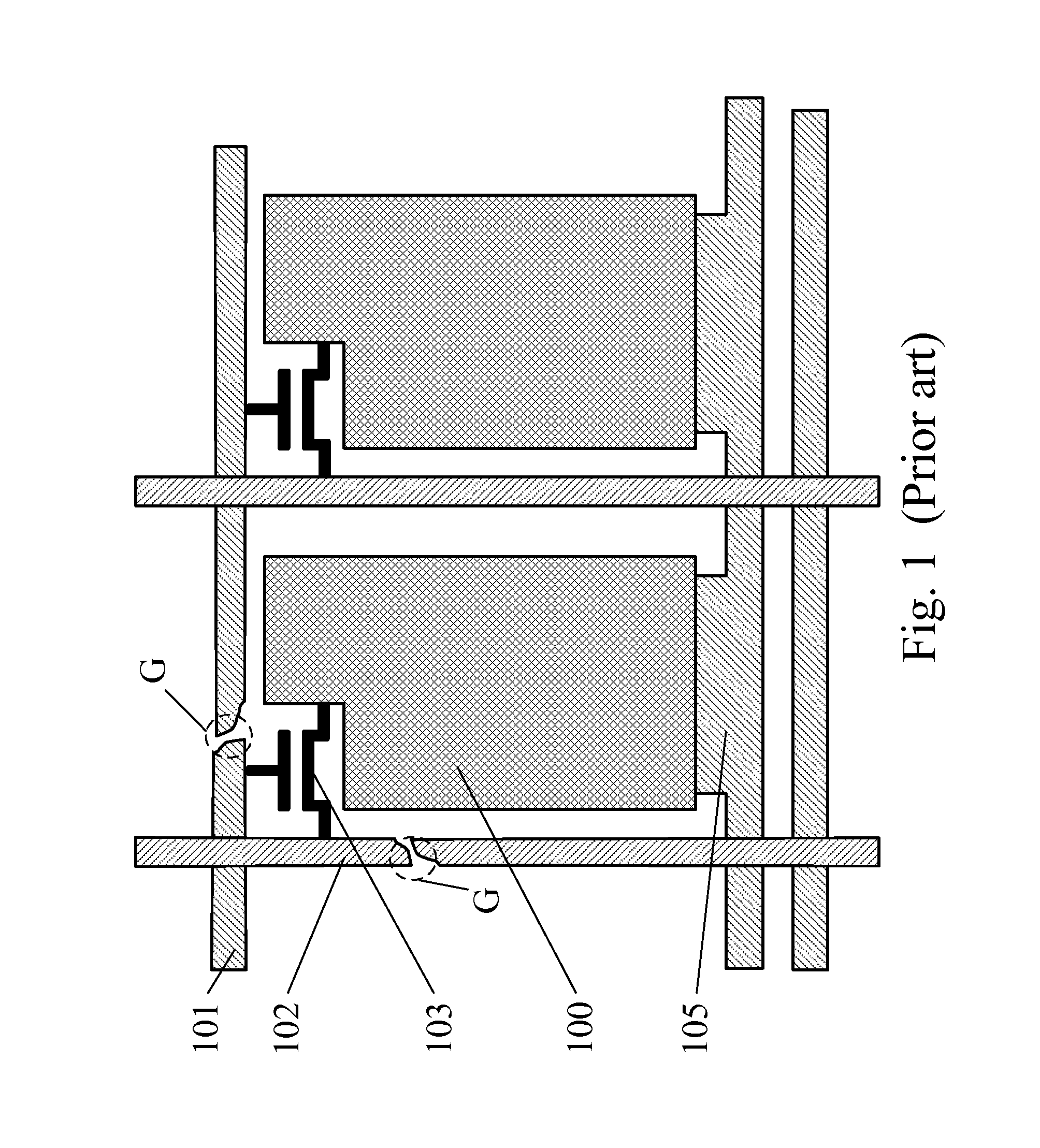
Otherwise, the LCD panel is scrapped nowadays if any of the data line 102 or the scan line 101 remains to be broken after cell processes are conducted, which causes unnecessary waste, affects the product yield, and increases the manufacturing cost of the LCD panel.

Method used


Image

  • Display panel and repair method thereof
  • Display panel and repair method thereof
  • Display panel and repair method thereof

Examples


first embodiment

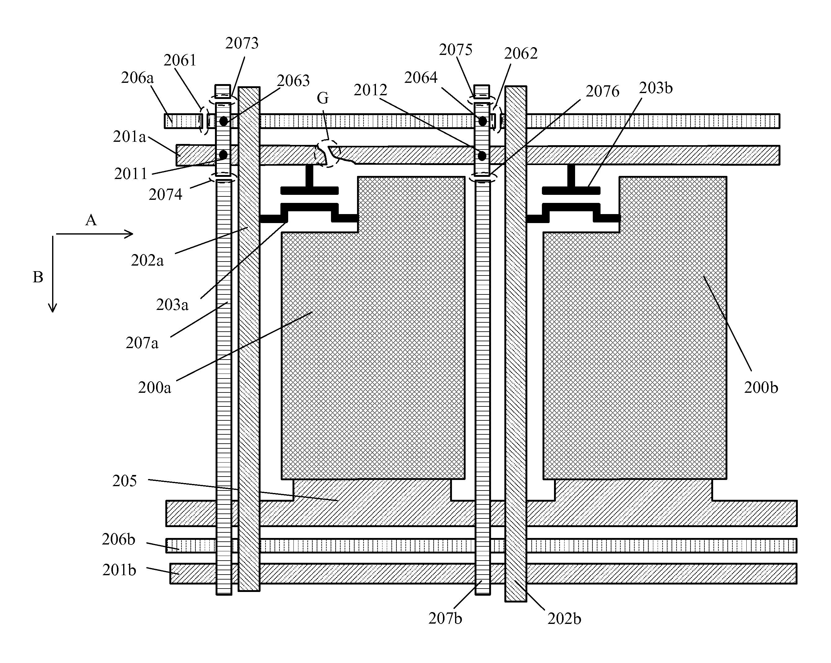
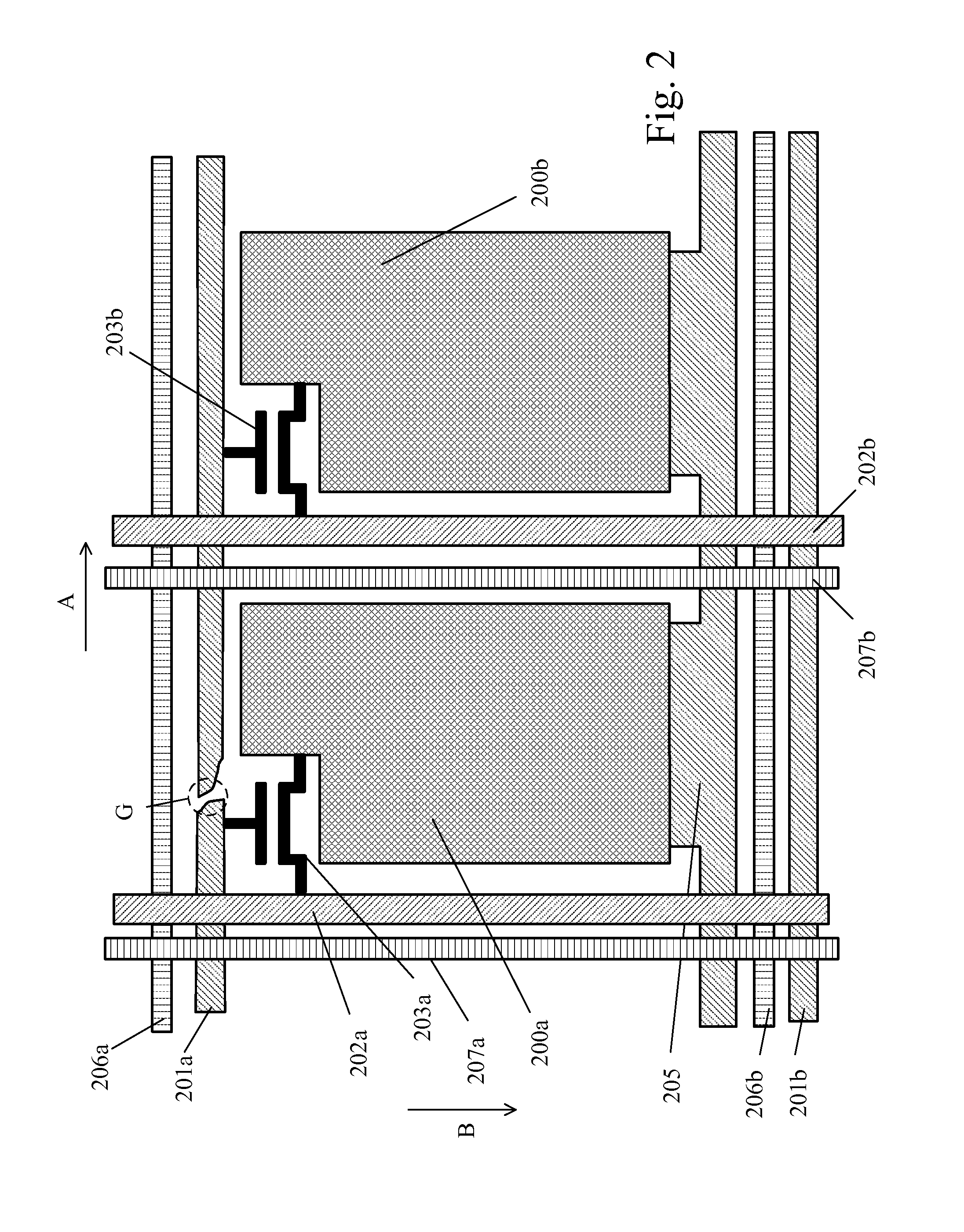
[0028]Refer to FIG. 3, which is a schematic diagram showing that the flat display panel in FIG. 2 has undergone repairs according to the present invention. If one of the plurality of scan lines 201a is probed to have the breaking the pixel electrode 200a cannot receive scan signals. At this time, any one of the plurality of horizontal repair lines is chosen as a first horizontal repair line, and any two of the plurality of vertical repair lines are chosen as a first and a second vertical repair line. In this embodiment, the horizontal repair line 206a is selected as a first horizontal repair line, and the vertical repair lines 207a and 207b are selected as a first and a second vertical repair line, respectively. Note that the first vertical repair line 207a and the second vertical repair line 207b have to be disposed on both sides of the pixel electrode 200a connected to the broken scan line 201a.

[0029]Afterwards, laser cutting is performed on the first horizontal repair line 206a ...

second embodiment

[0031]Refer to FIG. 4, which is a schematic diagram showing that the flat display panel in FIG. 2 has undergone repairs according to the present invention. The horizontal repair line 206b is chosen from the plurality of horizontal repair lines and is serves as a first horizontal repair line. The vertical repair lines 207a and 207c are chosen from the plurality of vertical repair lines and serve as a first and a second vertical repair line according to another embodiment. The first vertical repair line 207a and the second vertical repair line 207c have to be disposed on both sides of the pixel electrode 200a connected to the broken scan line 201a.

[0032]Afterwards, laser cutting is performed on the first horizontal repair line 206a to form a first cutting zone 2061 and a second cutting zone 2062. Laser cutting is also performed on the first vertical repair line 207a and the second vertical repair line 207c at both sides of the pixel electrode 200a to form a third cutting zone 2073 a...

third embodiment

[0037]Refer to FIG. 6, which is a schematic diagram showing that the flat display panel in FIG. 5 has undergone repairs according to the present invention. If one data lines 302a is found to have the breaking G; the pixel electrode 300a cannot receive data signals. At this time, any two of the plurality of horizontal repair lines are chosen as a first and a second horizontal repair line, and any one of the plurality of vertical repair lines is chosen as a first vertical repair line. In this embodiment, the horizontal repair lines 306a and 306b are selected as a first and a second horizontal repair line, and the vertical repair line 307a is selected as a first vertical repair line. The first horizontal repair lines 306a and the second horizontal repair line 306b have to be disposed on both sides of the pixel electrode 300a which is connected to the broken data line 302a.

[0038]Afterwards, laser cutting is performed on the first vertical repair line 307a to form a first cutting zone 3...


PUM


Abstract

A flat display panel and a related repairing method are provided. The flat display panel includes multiple horizontal repair lines parallel to scan lines and multiple vertical repair lines parallel to data lines. The vertical repair lines are disposed on one side of the data lines one to one, and the horizontal repair lines are disposed on one side of the scan lines one to one. When one of the data lines or one of the scan lines is broken, an electrical route formed by a use of the vertical repair lines or the horizontal repair lines detours the broken scan line or data line, so as to deliver signal to pixel electrode normally.

Description

BACKGROUND OF THE INVENTION[0001]1. Field of the Invention[0002]The present invention relates to a flat display panel and a repair method thereof, and more particularly, to a flat display panel with a structure having repair lines and a method of repairing broken lines thereof[0003]2. Description of the Prior Art[0004]An advanced monitor with multiple functions is an important feature for use in current consumer electronic products. Liquid crystal displays (LCDs) which are colorful monitors with high resolution are widely used in various electronic products such as monitors for mobile phones, personal digital assistants (PDAs), digital cameras, laptop computers, and notebook computers.[0005]A thin-film transistor liquid crystal display (TFT-LCD) panel has gradually become a mainstream product in the consumer electronics market because it has many advantages, such as high quality, efficient utilization of space, low consumption power, and no radiation. Refer to FIG. 1, which is a par...

Claims


Application Information

Patent Timeline
IPC IPC(8): G02F1/1343H01J9/50
CPCG02F1/136259G02F2001/136263G02F2001/136272G09G2300/08G09G2230/00G09G3/3648G02F2201/508G02F1/136263G02F1/136272
Inventor ZHUANG, YIZHUANGWEN, SONGXIANDENG, MINGFENG
Owner TCL CHINA STAR OPTOELECTRONICS TECH CO LTD
Learn More