Light emitting device package and manufacturing method thereof

a technology of light-emitting devices and manufacturing methods, which is applied in the direction of semiconductor/solid-state device manufacturing, semiconductor devices, electrical devices, etc., can solve the problems of deteriorating product reliability, reducing product productivity, and slowing down the development pace, so as to improve the correlated color temperature (cct)

Inactive Publication Date: 2012-12-06
SAMSUNG ELECTRONICS CO LTD
View PDF6 Cites 50 Cited by
  • Summary
  • Abstract
  • Description
  • Claims
  • Application Information

AI Technical Summary

Benefits of technology

[0018]An aspect of the present invention provides a method of manufacturing a light emitting device package having a color rendering index (CRI) of 90 or above, as well as improved correlated color temperature (CCT).

Problems solved by technology

In recent years, the primary characteristics of an LED chip itself have been rapidly enhanced, but at present, the development thereof has reached a certain technological level of development and the pace of development is therefore slowing.
However, when the white LED chip and the red LED chip are used at the same time, it is necessary to configure a separate circuit through feedback with respect to each of the white LED chip and the red LED chip, whereby productivity may be reduced.
In the related art, phosphor application thickness and amount have been adjusted for each product, and accordingly, non-uniform thicknesses thereof have been caused to thereby deteriorate product reliability and make the characteristics of light different in each product, causing a decline in product quality.
In the related art, whenever the power of chips has been altered, it has been cumbersome to adjust both the amount of phosphors in a red second wavelength conversion part and the amount of phosphors in a green second wavelength conversion part.
In the case of the application of phosphor materials by a dispensing process, the thickness of the outermost phosphor layer may be entirely uneven, so color deviation in light emitted from the LED chip may occur, resulting in a reduction of product reliability.
Accordingly, a highly advanced phosphor application technique is required, thereby resulting in a low yield, and thus a product manufacturing time and manufacturing costs may be increased.

Method used


Image

  • Light emitting device package and manufacturing method thereof
  • Light emitting device package and manufacturing method thereof
  • Light emitting device package and manufacturing method thereof

Examples


Embodiment Construction

[0069]Embodiments of the present invention will now be described in detail with reference to the accompanying drawings.

[0070]The invention may, however, be embodied in many different forms and should not be construed as being limited to the embodiments set forth herein. Rather, these embodiments are provided so that this disclosure will be thorough and complete, and will fully convey the scope of the invention to those skilled in the art.

[0071]In the drawings, the shapes and sizes of elements may be exaggerated for clarity, and the same reference numerals will be used throughout to designate the same or like elements.

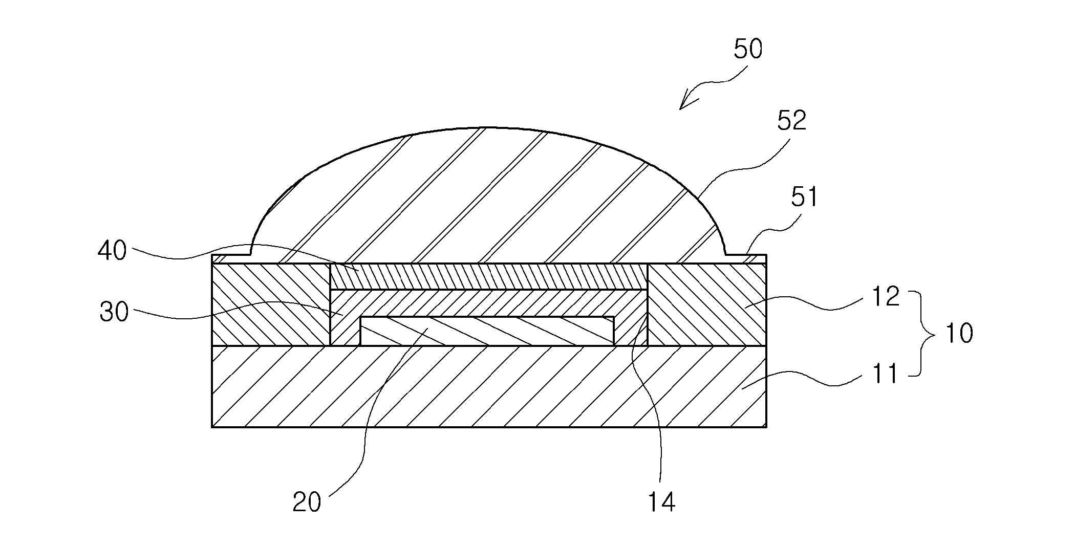
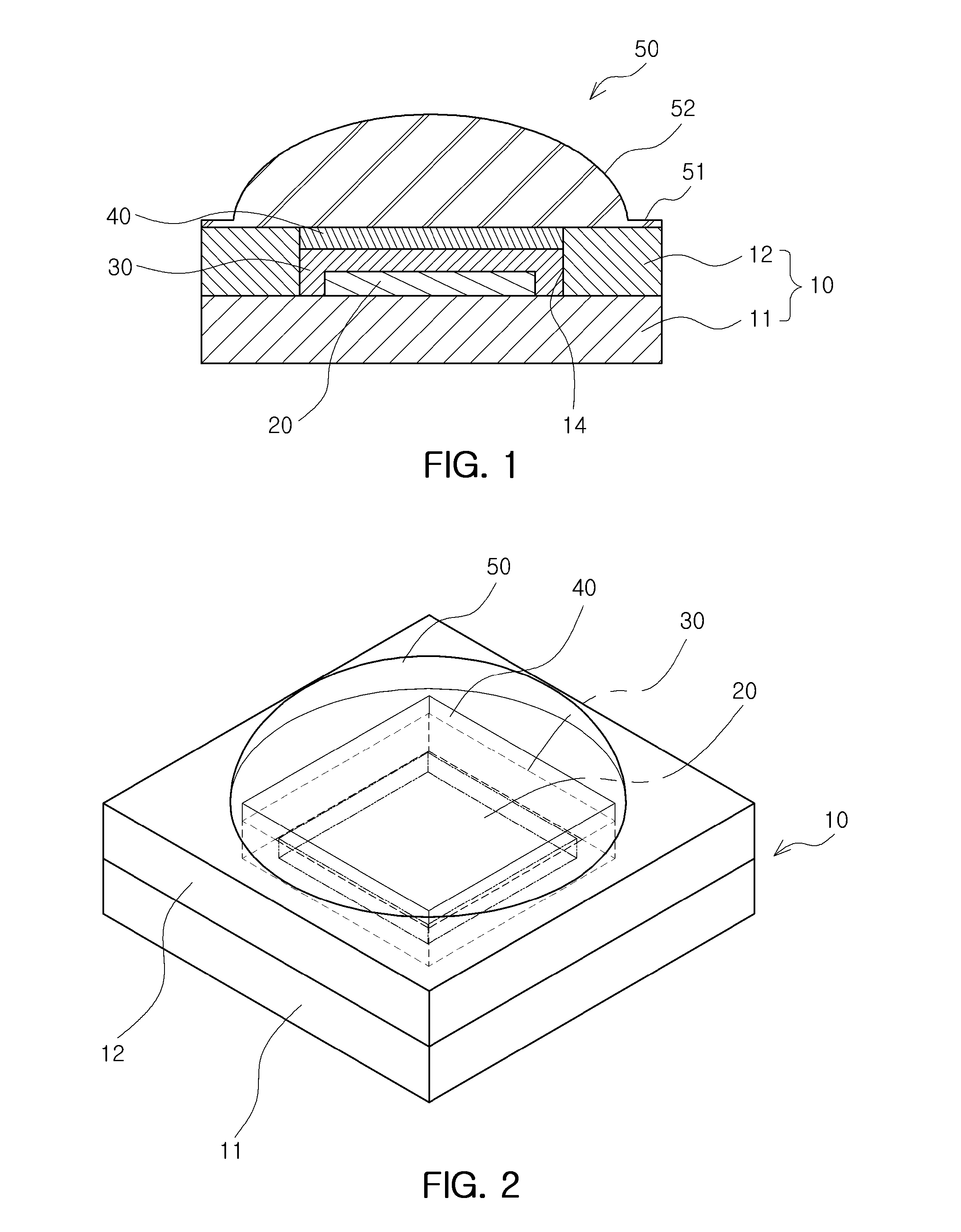
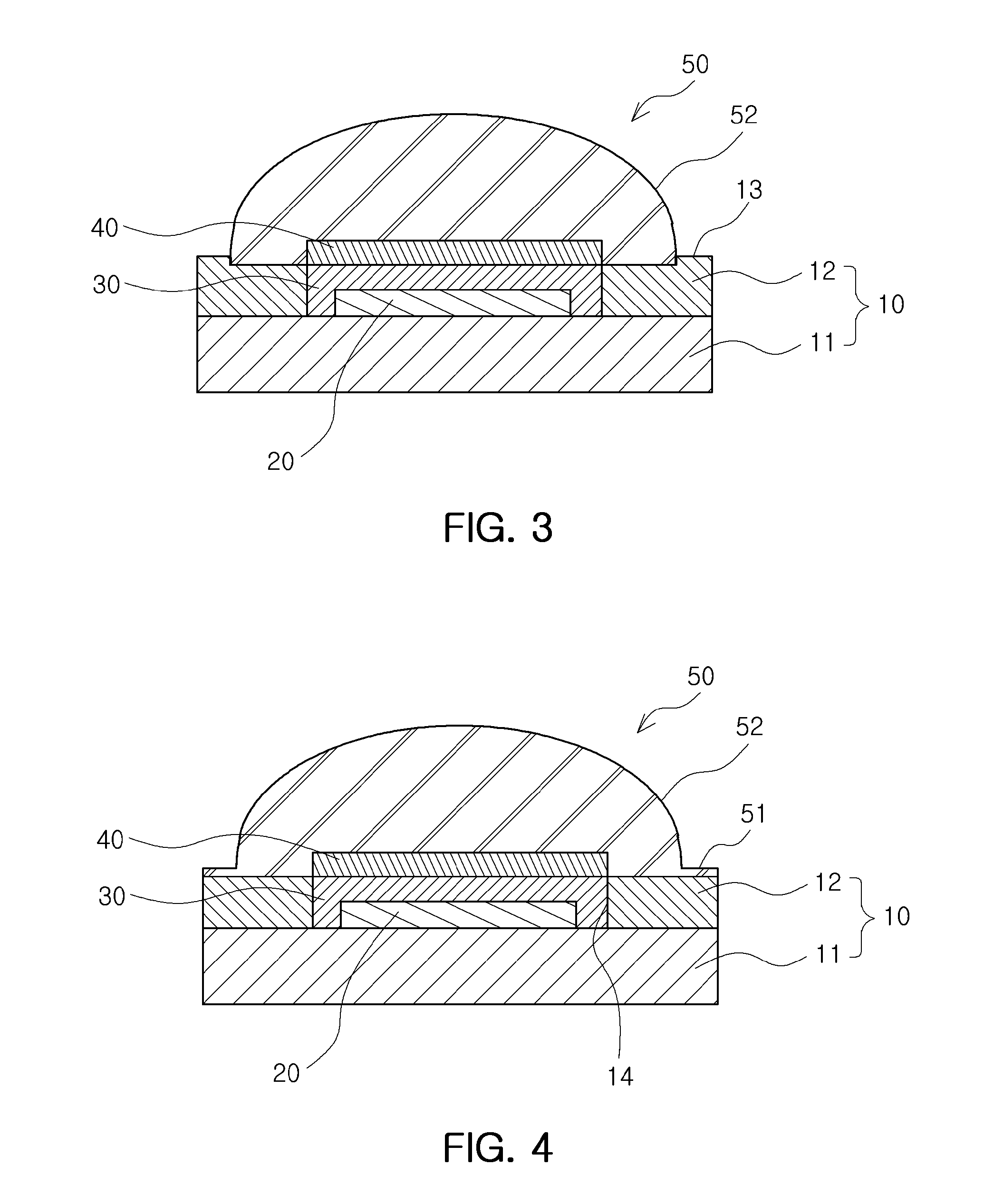
[0072]With reference to FIGS. 1 and 2, a light emitting device package according to an embodiment of the present invention includes a substrate 10 having a cavity 14 formed therein, a light emitting device 20 mounted on a bottom surface of the cavity 14 of the substrate 10, a first wavelength conversion part 30 dispensed to cover the light emitting device 20 within the ...


PUM


Abstract

There is provided a light emitting device package including a substrate having a cavity therein; alight emitting device mounted on a bottom surface of the cavity; a first wavelength conversion part including a first phosphor for a wavelength conversion of light emitted from the light emitting device and covering the light emitting device within the cavity; and a second wavelength conversion part including a second phosphor allowing for emission of light having a wavelength different to that of the first phosphor and formed as a sheet on the first wavelength conversion part.

Description

CROSS-REFERENCE TO RELATED APPLICATIONS[0001]This application claims the priority of Korean Patent Application No. 10-2011-0053239 filed on Jun. 2, 2011, in the Korean Intellectual Property Office, the disclosure of which is incorporated herein by reference.BACKGROUND OF THE INVENTION[0002]1. Field of the Invention[0003]The present invention relates to a light emitting device package and a method of manufacturing the same.[0004]2. Description of the Related Art[0005]A light emitting diode (LED) is a semiconductor device capable of emitting light of various colors, due to electron-hole recombination occurring at a p-n junction when a current is supplied thereto, by using compound semiconductor materials such as GaAs, AlGaAs, GaN, InGaN, AlGaInP and the like as a light source.[0006]LEDs are environmentally-friendly, have fast response rates on the level of several nano seconds so as to be effective for a video signal stream, and are capable of being impulsively driven.[0007]Moreover, ...

Claims


Application Information

Patent Timeline
Patent Type & Authority Applications(United States)
IPC IPC(8): H01L33/44H01L33/58
CPCH01L33/504H01L33/507H01L33/58H01L33/60H01L2924/0002H01L2924/00H01L33/50
Inventor KIM, HYUNG KUN
Owner SAMSUNG ELECTRONICS CO LTD
Why Eureka
Try Eureka