High frequency interconnect structures, electronic assemblies that utilize high frequency interconnect structures, and methods of operating the same

a high-frequency interconnect and electronic assembly technology, applied in the high-frequency field, can solve the problems of ineffectiveness at frequencies greater than approximately 20 gigahertz (ghz), ineffective packing/or crosstalk among a plurality of optical fibers within optical interconnects, etc., to achieve the effect of reducing the potential for crosstalk

Active Publication Date: 2012-12-06
FORMFACTOR INC
View PDF5 Cites 554 Cited by
  • Summary
  • Abstract
  • Description
  • Claims
  • Application Information

AI Technical Summary

Benefits of technology

[0005]High frequency interconnect structures, electronic assemblies that utilize high frequency interconnect structures, and methods of operating the same. The high frequency interconnect structures include a plurality of dielectric waveguides and are configured to communicatively connect a plurality of transmitters with a plurality of receivers and to convey a plurality of signals therebetween. The plurality of signals may include a plurality of electromagnetic waves and may have a frequency of at least 200 GHz. The high frequency interconnect structures further may be configured to decrease a potential for crosstalk between a first signal that is conveyed by a first dielectric waveguide of the plurality of dielectric waveguides and a second signal that is conveyed by a second dielectric waveguide of the plurality of dielectric waveguides. The high frequency interconnect structures may provide this decreased potential for crosstalk through control of a passband of the first dielectric waveguide relative to a passband of the second dielectric waveguide and / or the use of a crosstalk mitigation structure.

Problems solved by technology

These electrical interconnects, while effective over a range of data transmission rates, which also may be referred to herein as bit rates and / or frequencies, may be ineffective at frequencies that are greater than approximately 20 gigahertz (GHz) due to transmission line losses, dispersion, impedance mismatches, and / or electromagnetic crosstalk.
While a maximum frequency of these electrical interconnects may be increased to some extent, such as through the use of equalization techniques, implementing these equalization techniques requires additional system complexity, expense, and / or space within the electronic assemblies.
However, effective packing of the optical fibers within optical interconnects, and / or crosstalk among a plurality of optical fibers within the optical interconnects, may be problematic.
These conversion devices typically consume a significant amount of power, are expensive to design and / or construct, are relatively large, and / or may require mixing different semiconductor technologies.

Method used


Image

  • High frequency interconnect structures, electronic assemblies that utilize high frequency interconnect structures, and methods of operating the same
  • High frequency interconnect structures, electronic assemblies that utilize high frequency interconnect structures, and methods of operating the same
  • High frequency interconnect structures, electronic assemblies that utilize high frequency interconnect structures, and methods of operating the same

Examples


Embodiment Construction

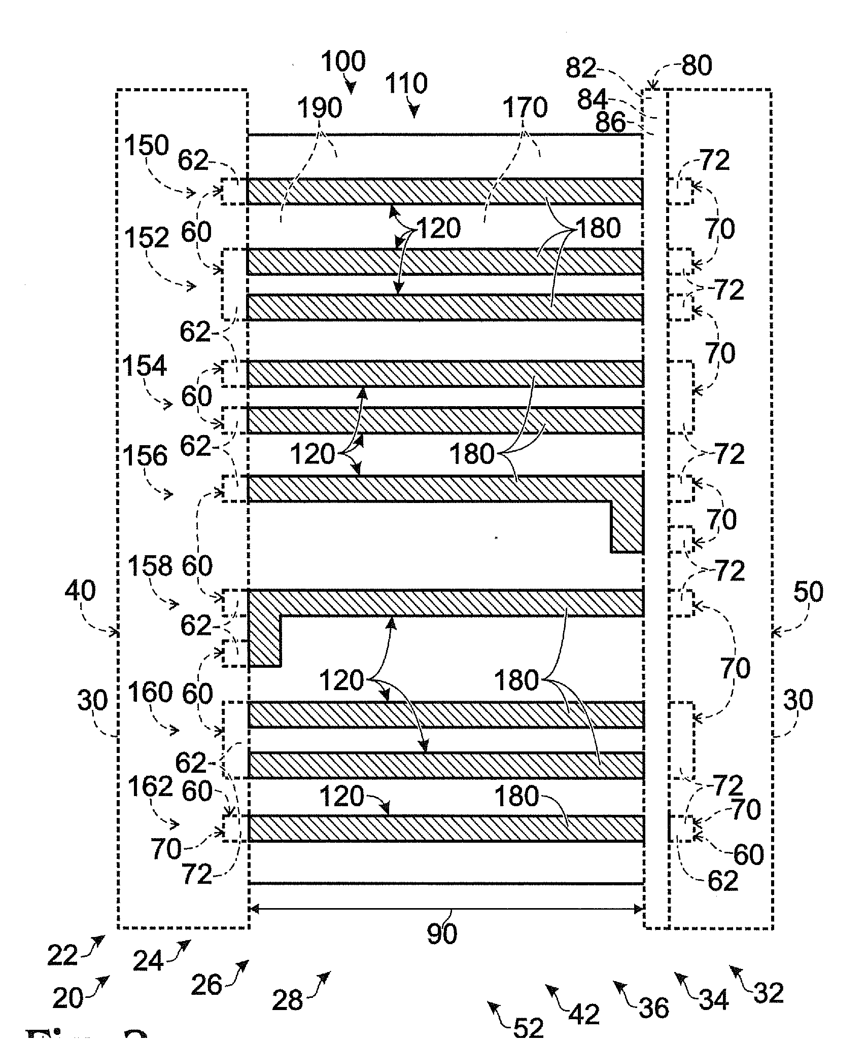
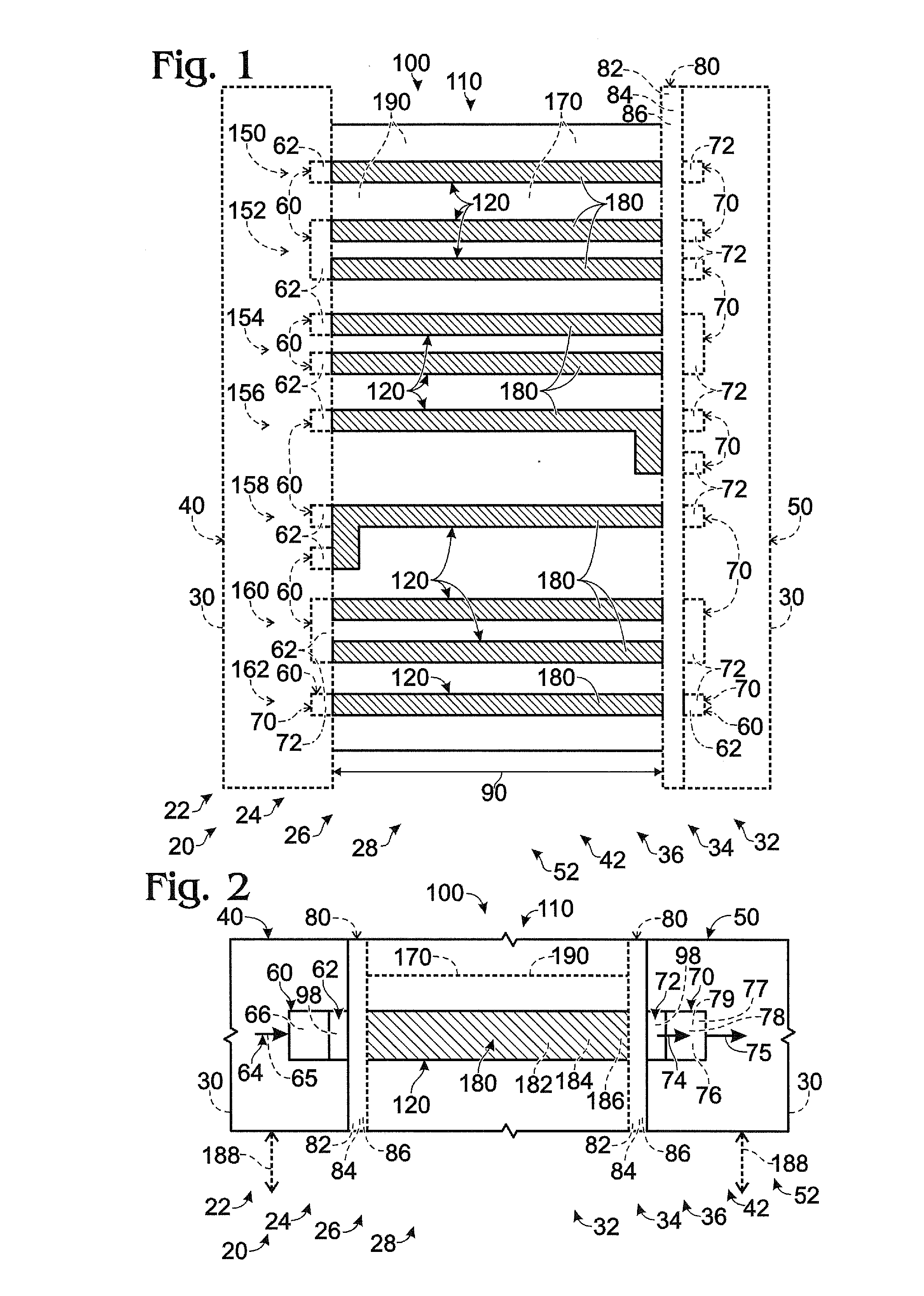
[0017]FIG. 1 is a schematic representation of illustrative, non-exclusive examples of a high frequency interconnect structure 100 that includes a plurality of dielectric waveguides 120 according to the present disclosure, while FIG. 2 is a schematic representation of a portion of the high frequency interconnect structure of FIG. 1. FIGS. 1 and 2 will be discussed in parallel herein and illustrate features and / or components that may be included in high frequency interconnect structure 100, as well as assemblies that may include high frequency interconnect structures 100 according to the present disclosure. While a particular feature, component, and / or assembly may not be illustrated in both of FIGS. 1 and 2, it is within the scope of the present disclosure that any of the high frequency interconnect structures that are discussed herein may include any and / or all of the features and / or components and / or may be included an any of the assemblies that are discussed herein.

[0018]As shown ...


PUM


Abstract

High frequency interconnect structures, electronic assemblies that utilize high frequency interconnect structures, and methods of operating the same. The high frequency interconnect structures include a plurality of dielectric waveguides and are configured to communicatively connect a plurality of transmitters with a plurality of receivers and to convey a plurality of signals therebetween. The plurality of signals may include a plurality of electromagnetic waves and may have a frequency of at least 200 GHz. The high frequency interconnect structures further may be configured to decrease a potential for crosstalk between a first signal that is conveyed by a first dielectric waveguide of the plurality of dielectric waveguides and a second signal that is conveyed by a second dielectric waveguide of the plurality of dielectric waveguides, such as through control of a passband of the first dielectric waveguide relative to the second dielectric waveguide and / or the use of a crosstalk mitigation structure.

Description

RELATED APPLICATION[0001]This application claims priority to U.S. Provisional Patent Application Ser. No. 61 / 493,314, which is entitled “High Frequency Interconnection,” was filed on Jun. 3, 2011, and the complete disclosure of which is hereby incorporated by reference.FIELD OF THE DISCLOSURE[0002]The present disclosure is directed generally to high frequency interconnect structures and more particularly to high frequency interconnect structures that include a plurality of dielectric waveguides.BACKGROUND OF THE DISCLOSURE[0003]As the operating speed, or frequency, of electronic devices increases, there is an ever increasing demand for higher speed, lower cost, lower power, and / or lower overhead interconnects between and / or within electronic assemblies. Traditionally, electrical connections between pairs of terminals have been utilized to form electrical interconnects between electronic circuits. These electrical interconnects, while effective over a range of data transmission rates...

Claims


Application Information

Patent Timeline
Patent Type & Authority Applications(United States)
IPC IPC(8): H01P5/12
CPCH01P3/16H01P3/18G01R23/02
Inventor STRID, ERIC W.CAMPBELL, RICHARD L.SMITH, KENNETH R.GLEASON, K. REEDJUNG, KOOHO
Owner FORMFACTOR INC
Why Eureka
Try Eureka