Apparatus for displaying and sensing images

a technology of apparatus and image, applied in the field of apparatus for integrated capture and display, can solve the problems of reducing the resolution of formed images, deteriorating the quality of images captured, and prior art image capture and display systems typically suffer from reduced image quality, so as to achieve sufficient optical axis length, reduce overall thickness of apparatus, and improve imaging quality

Active Publication Date: 2012-12-06
GLOBAL OLED TECH
View PDF15 Cites 43 Cited by
  • Summary
  • Abstract
  • Description
  • Claims
  • Application Information

AI Technical Summary

Benefits of technology

[0023]An advantage of the present invention is that by locating lenses within or upon a transparent cover of an integrated display and image sensing apparatus, the overall thickness of the apparatus can be reduced while, at the same time, maintaining a sufficiently long optical axis to provide improved imaging quality. Fewer separate elements are required, reducing complexity and cost. A high level of circuit integration in chiplets provides improved display image quality and opportunity for high-resolution image sensor arrays, as well as a multiplicity of imaging sensor arrays that enable the capture of a variety of images and video sequences having different attributes. For example, bandwidth can be reduced by performing high-resolution captures of only the important areas of a scene and low-resolution captures of the rest of the scene. Three-dimensional information or, in some embodiments, stereo capture can be easily performed without requiring either complicated lens or mirror structures.
is that by locating lenses within or upon a transparent cover of an integrated display and image sensing apparatus, the overall thickness of the apparatus can be reduced while, at the same time, maintaining a sufficiently long optical axis to provide improved imaging quality. Fewer separate elements are required, reducing complexity and cost. A high level of circuit integration in chiplets provides improved display image quality and opportunity for high-resolution image sensor arrays, as well as a multiplicity of imaging sensor arrays that enable the capture of a variety of images and video sequences having different attributes. For example, bandwidth can be reduced by performing high-resolution captures of only the important areas of a scene and low-resolution captures of the rest of the scene. Three-dimensional information or, in some embodiments, stereo capture can be easily performed without requiring either complicated lens or mirror structures.

Problems solved by technology

This is difficult, however, since a communicating individual will tend to look at the display while addressing the remote individual, thus giving the appearance that the individual is not looking at the person to whom he or she is speaking
In other cases, a lens element is located very close to, or on, an imaging element which can deteriorate the quality of the images captured.
In other cases, relatively few image sensing elements are provided, reducing the resolution of the formed images.
Hence, prior art image capture and display systems typically suffer from reduced image quality (e.g. resolution and sharpness) or are thicker than can be desirable.
Thin-film transistors made from amorphous or polycrystalline silicon are relatively larger and have lower performance than conventional transistors made from crystalline silicon wafers.
Moreover, such thin-film devices typically exhibit local or large-area non-uniformity that results in perceptible non-uniformity in a display employing such materials.
While improvements in manufacturing and materials processes are made, the manufacturing processes are expensive and thin-film device performance continues to be lower than the performance of crystalline silicon devices.
These disclosures, however, do not provide an integrated image capture and display apparatus.

Method used


Image

  • Apparatus for displaying and sensing images
  • Apparatus for displaying and sensing images
  • Apparatus for displaying and sensing images

Examples


Embodiment Construction

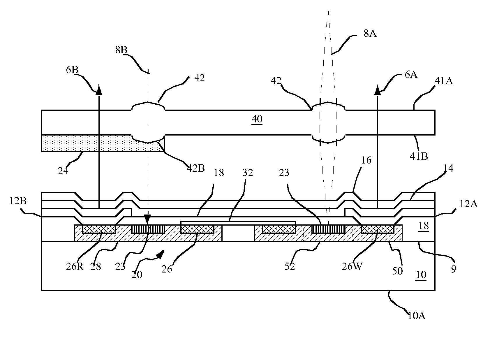
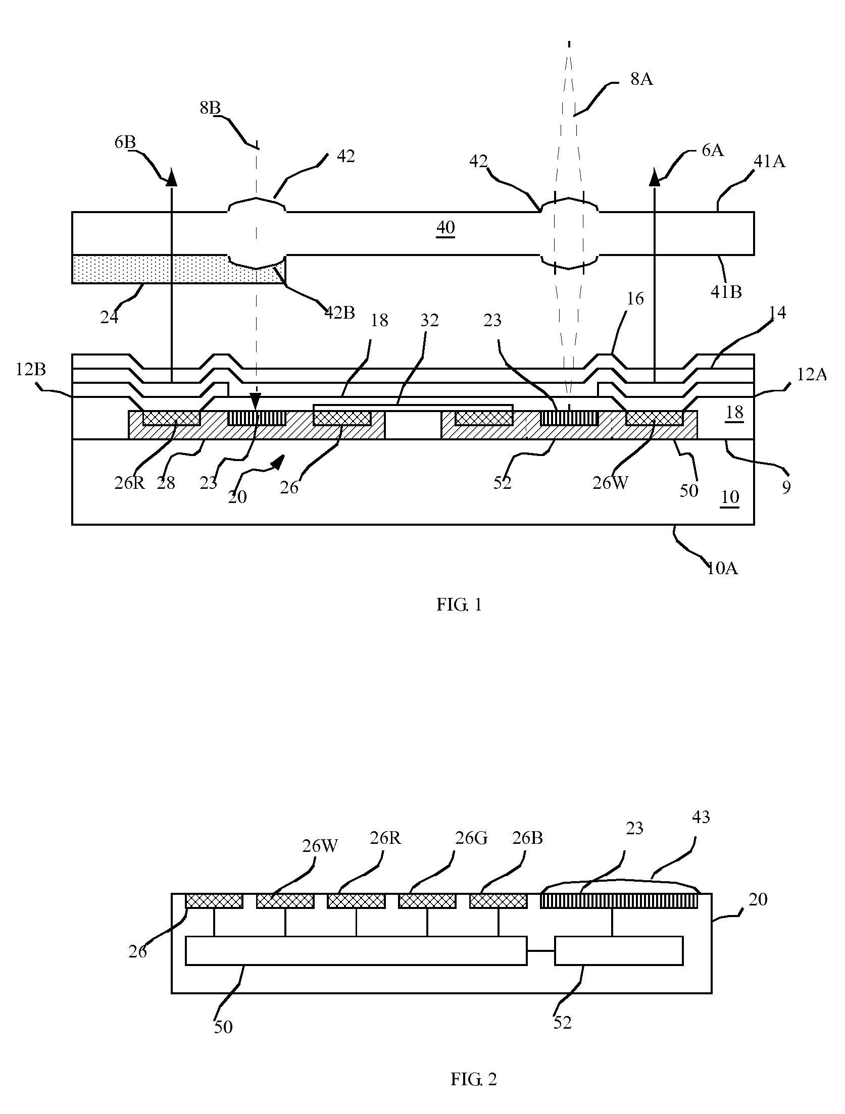
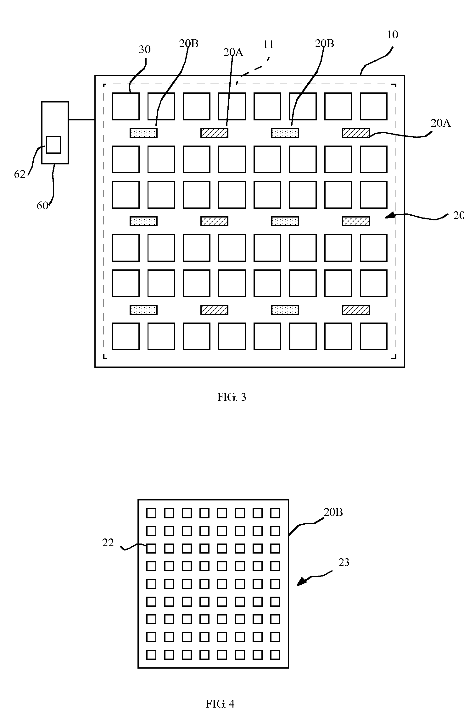
[0038]Referring to FIGS. 1-3, an apparatus for displaying and sensing images comprises a display substrate 10 having a display area 11 on a device side 9 of the display substrate 10. A plurality of pixels 30 (FIG. 3) is located in the display area 11 on the device side 9 of the display substrate 10, each pixel 30

[0039](FIG. 3) including a control electrode 12A, 12B spaced apart from a transparent electrode 16, and at least one layer 14 of light-emitting material located between the control electrode 12A, 12B and the transparent electrode 16. A plurality of chiplets 20 each providing pixel control, to at least one pixel and having a chiplet substrate 28 independent of the display substrate 10 is located over, and affixed to, the device side 9 of the display substrate 10 in the display area 11, each chiplet 20 providing pixel control having at least one connection pad 26 and at least one pixel control circuit 50. The pixel control circuit 50 (FIG. 2) is electrically connected to the c...


PUM


Abstract

An apparatus for displaying and sensing images includes a display substrate and a plurality of electroluminescent pixels. A plurality of pixel control chiplets and one or more sensor chiplets are affixed to the device side of the display substrate in the display area. A transparent cover is spaced apart from and affixed to the device side of the display substrate, and has a plurality of imaging lenses formed on or in it, each imaging lens spaced apart from and corresponding to an image sensor array in a sensor chiplet for forming an imaging plane on the corresponding image sensor array.

Description

CROSS REFERENCE TO RELATED APPLICATIONS[0001]Reference is made to commonly-assigned, co-pending U.S. patent application Ser. No. 12 / 191,478, filed Aug. 14, 2008, entitled “OLED device with embedded chip driving” by Winters et al and to commonly-assigned co-pending U.S. patent application Ser. No. 12 / 608,049, filed Oct. 29, 2009, entitled “ACTIVE MATRIX ELECTROLUMINESCENT DISPLAY WITH SEGMENTED ELECTRODE”, the disclosures of which are incorporated herein by reference.FIELD OF THE INVENTION[0002]The present invention relates to apparatus for integrated capture and display that provides both image display and image capture functions.BACKGROUND OF THE INVENTION[0003]Flat-panel display devices are widely used in conjunction with computing devices, in portable devices, and for entertainment devices such as televisions. Such displays typically employ a plurality of pixels distributed over a substrate to display images. Each pixel incorporates several, differently colored light-emitting ele...

Claims


Application Information

Patent Timeline
Patent Type & Authority Applications(United States)
IPC IPC(8): H04N5/225
CPCH01L27/14603H01L27/3227H01L27/14643H10K59/60H01L27/14627H10K59/129
Inventor COK, RONALD S.ARNOLD, ANDREWMILLER, MICHAEL E.HAMER, JOHN W.
Owner GLOBAL OLED TECH
Why Eureka
Try Eureka