Integrated touch panel structure and manufacturing method thereof

a touch panel and integrated technology, applied in the field of integrated touch panel structure and manufacturing method thereof, can solve the problems of difficult adjustment of touch signal, increased resistance between connectors and cables, and enlarged noise, so as to reduce reduce the effect of electromagnetic interference of sensing signals, and effectively separate circuit components from elements

a touch panel and integrated technology, applied in the field of integrated touch panel structure and manufacturing method thereof, can solve the problems of difficult adjustment of touch signal, increased resistance between connectors and cables, and enlarged noise, so as to reduce reduce the effect of electromagnetic interference of sensing signals, and effectively separate circuit components from elements

US20120313863A1Inactive Publication Date: 2012-12-13HANNSTAR DISPLAY CORPORATION

Image

  • Integrated touch panel structure and manufacturing method thereof
  • Integrated touch panel structure and manufacturing method thereof
  • Integrated touch panel structure and manufacturing method thereof

Examples


Embodiment Construction

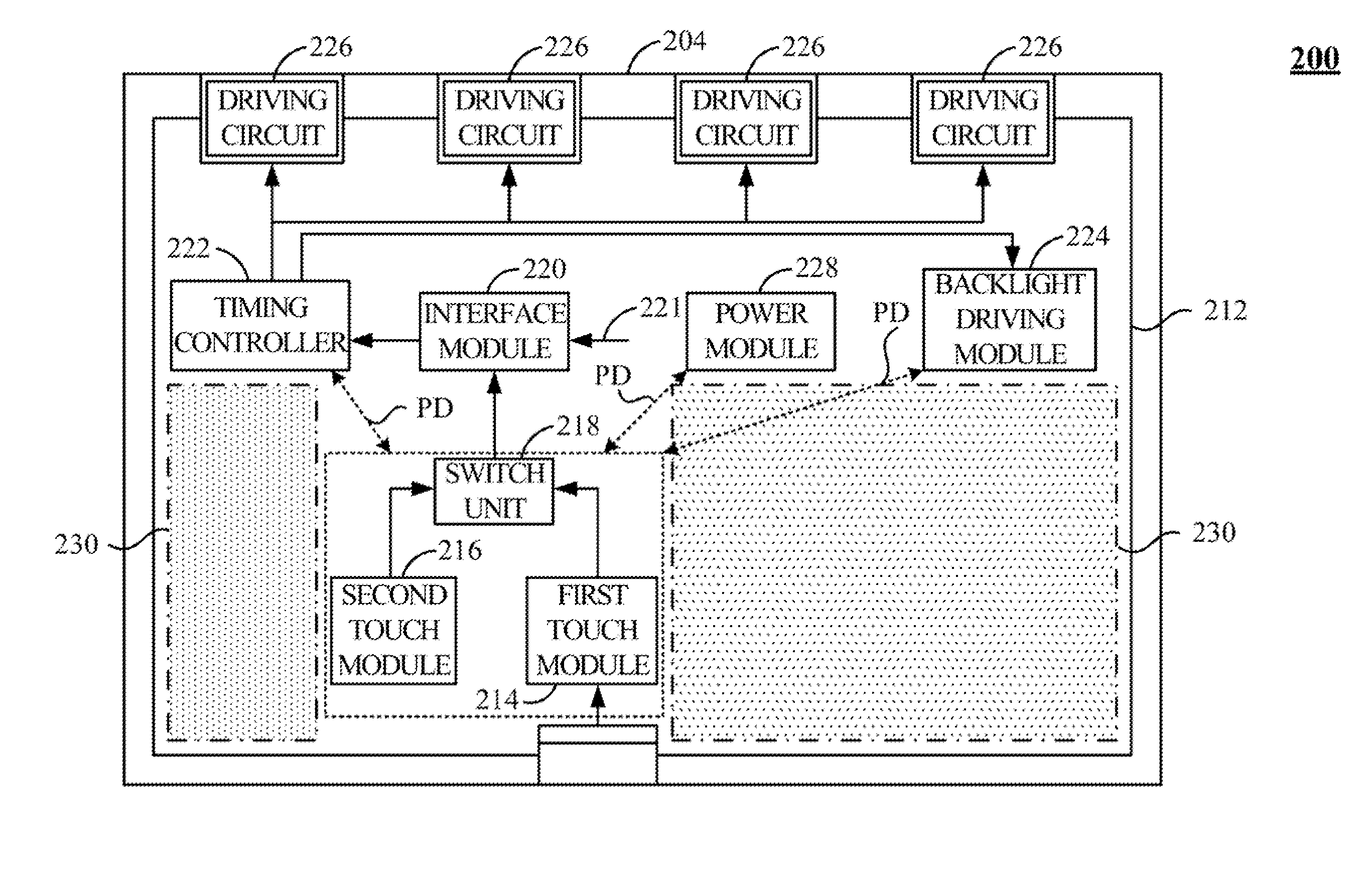
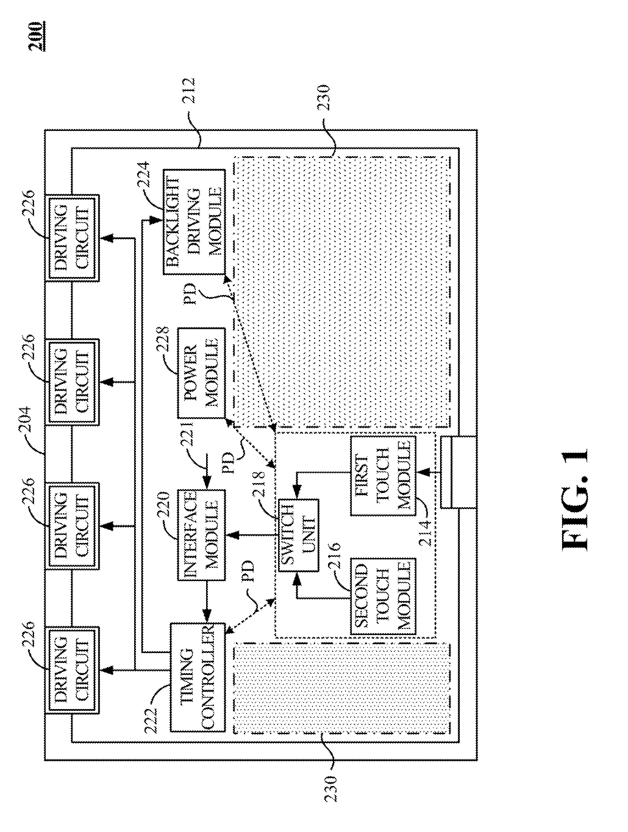
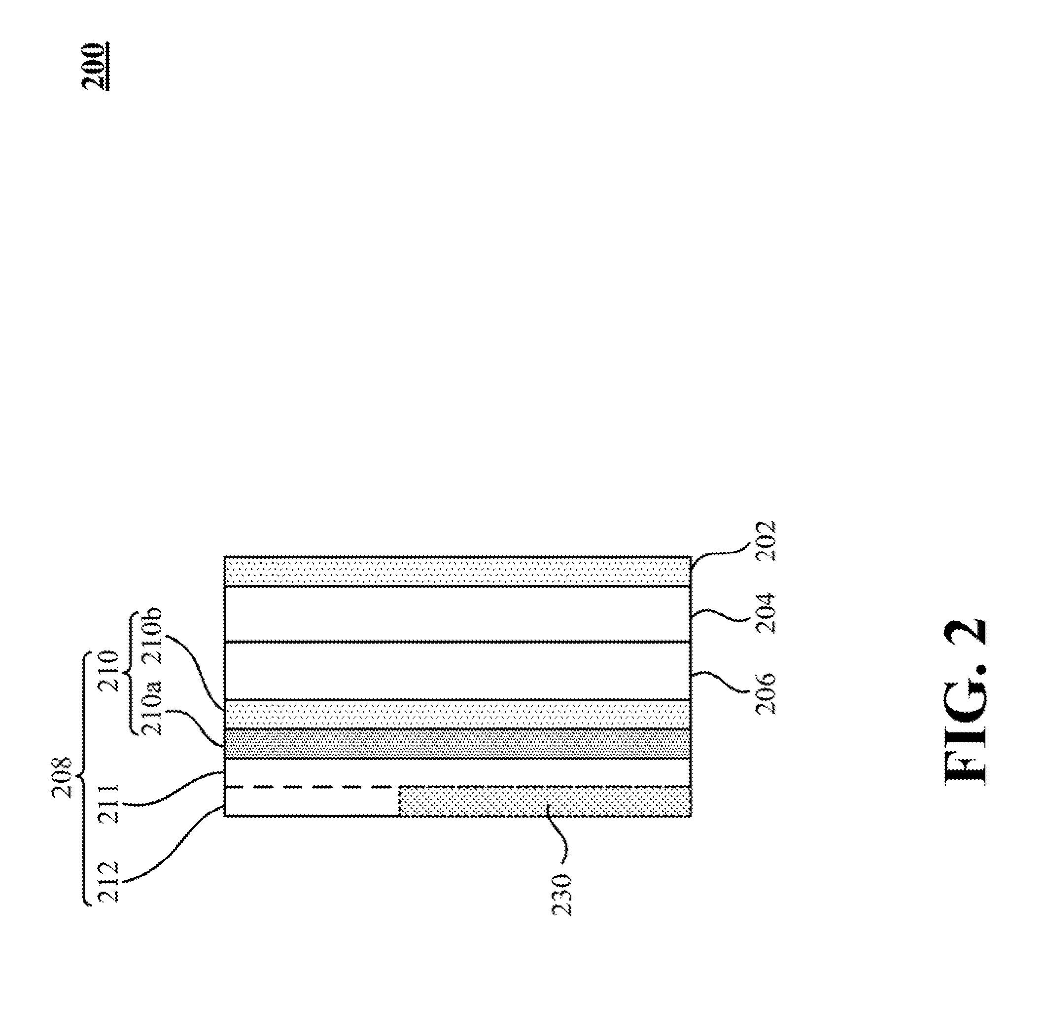
[0022]Please refer to FIG. 1 and FIG. 2. FIG. 1 is a schematic top view of an integrated touch panel structure 200 according to one embodiment of the present invention. FIG. 2 is a schematic side view of the integrated touch panel structure 200 according to one embodiment of the present invention. The integrated touch panel structure 200 includes a first sensing layer 202, a displaying layer 204, a backlight plate 206 and a composite component layer 208. The first sensing layer 202 generates a first sensing signal for sensing the touch operation of user's finger on the first sensing layer 202. In one case, the first sensing layer 202 is a capacitive type touch board. For example, the capacitive type touch board is an indium tin oxide (ITO) layer. The displaying layer 204 displays a program execution window wherein the first sensing layer 202 is disposed on a first side-wall of the displaying layer 204. The first sensing layer 202 generates the first sensing signal corresponding to a...


PUM

PropertyMeasurementUnit
areaaaaaaaaaaa
distanceaaaaaaaaaa
electromagneticaaaaaaaaaa

Abstract

An integrated touch panel structure and manufacturing method thereof are described. The integrated touch panel structure is integrated by a first sensing layer, a displaying layer, a backlight plate and a composite component layer. The composite component layer includes a second sensing layer and a processing circuit layer. The processing circuit layer further includes a metal area for preventing a touch signal from electromagnetic interference to increase the precision of the touch signal.

Description

FIELD OF THE INVENTION[0001]The present invention relates to a touch panel structure and method thereof, and more particularly to an integrated touch panel structure and manufacturing method thereof for integrating a first sensing layer, a displaying layer, a backlight plate and a composite component layer wherein the composite component layer has a second sensing layer and a processing circuit layer.BACKGROUND OF THE INVENTION[0002]With the rapid development of information technology, many electronic products widely currently utilizes touch technology as a manner of message input and the user can read or browse the information on the display panel or transmit the input message when the user touches the display panel by finger or stylus pen, which replace the manner of keypad or keyboard installed in the conventional electronic products. For example, touch panel has been a rush-developing market for several manufacturers due to the incitation of IPhone's great demand in the cell pho...

Claims


Application Information

Patent Timeline
13 Dec 2012
Publication
US20120313863A1
IPC
G06F3/041; H05K13/00
CPC
G06F3/0412; Y10T29/49002; G06F2203/04103; G06F3/044; G06F3/0445
Inventors
HSU, FU-TSENG