Integrated touch screen

Active Publication Date: 2012-12-13
LG INNOTEK CO LTD
View PDF15 Cites 36 Cited by
  • Summary
  • Abstract
  • Description
  • Claims
  • Application Information

AI Technical Summary

Benefits of technology

[0014]In accordance with exemplary embodiments of the present invention, the integrated touch window is advantageous that the strength of a whole touch sensor module can be improved and a process can be simplified by integrally impl

Problems solved by technology

However, when the touch screen panel is attached to an upper part of a panel of the image display unit, a whole volume of the image display unit increases, so a problem such as the degradation in convenience to carry out may occur.
Thus, this is disadvantageous that the touch screen panel increases in thickness, thereby going counter to the trend toward a thinner touch screen panel.
The production of the touch screen panel using the window of each cell unit is disad

Method used


Image

  • Integrated touch screen
  • Integrated touch screen
  • Integrated touch screen

Examples


Example

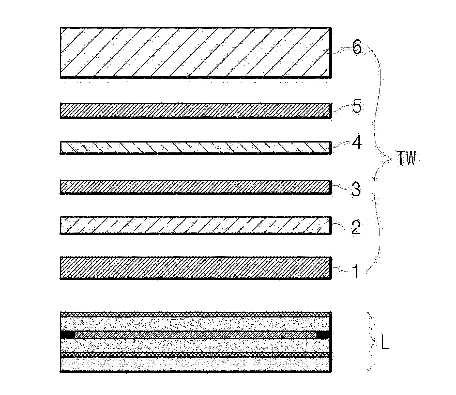
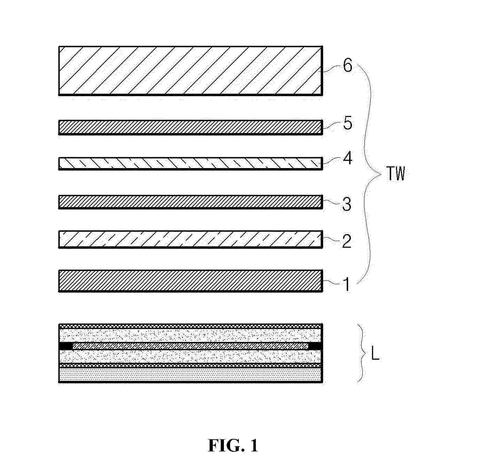
(1) FIRST EXEMPLARY EMBODIMENT

[0028]A structure according to this exemplary embodiment is explained with an example which implements in detail the structure of FIG. 2. That is, as illustrated in FIG. 3, a touch sensor module may be formed in the structure including base substrates 130 and 110, and sensing electrodes 132 and 112 patterned on one surface of the base substrate or on other surface opposed to the one surface. That is, the touch sensor module may include: a first sensing electrode pattern layer 130 bonded to the transparent window 100 via a first adhesive material layer 140, and having the sensing electrode pattern 132 on one surface; and a second sensing electrode pattern layer 110 bonded to other surface of the first sensing electrode pattern layer via a second adhesive material layer 120, and having the sensing electrode pattern 112 on one surface. In particular, in this case, the first sensing electrode pattern 132 and the second sensing electrode pattern 112 may be ...

Example

(2) SECOND EXEMPLARY EMBODIMENT

[0030]Unlike the structure of FIG. 3, but like the structure of FIG. 4, when implementing the sensor electrode pattern layer, the sensing electrode 232 pattern is formed on both surfaces of the base substrate 230. In view of this, there is a difference between the structures. Moreover, a protective film 210 for protecting the sensing electrode pattern of a lower surface of the base substrate 230 may be further included.

Example

(3) THIRD EXEMPLARY EMBODIMENT

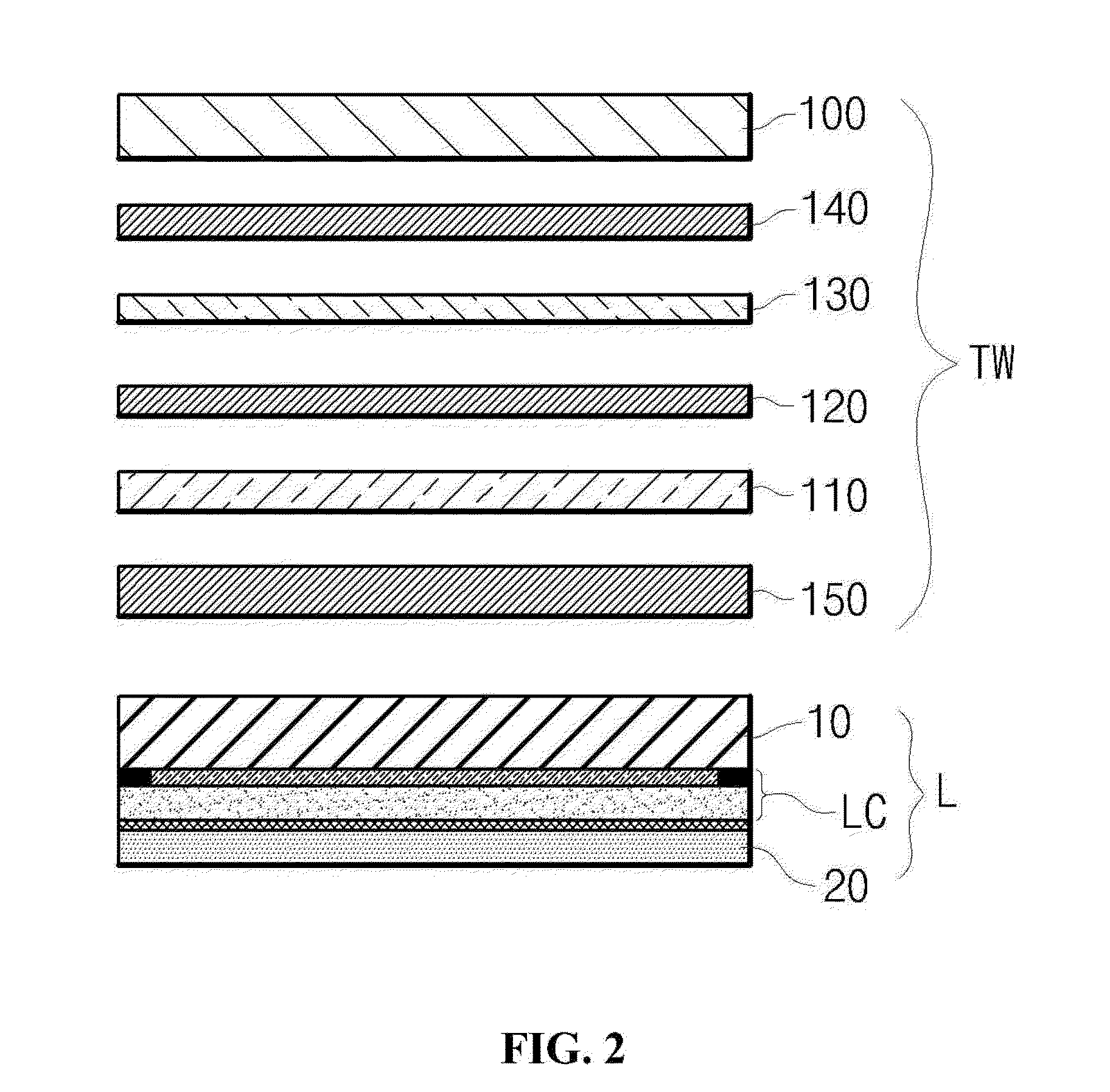
[0031]Explaining a structure of the third exemplary embodiment with reference to FIG. 5, FIG. 4 illustrates other structure of the sensing electrode pattern layer according to still another exemplary embodiment of the present invention. That is, a transparent window 300 is formed, a sensing electrode pattern 312 is patterned on a sectional surface of a base substrate 310, and a wiring part 311 is simultaneously formed with the sensing electrode pattern. The first and second sensing electrode patterns are implemented on the same plane as each other. The first sensing electrode layer for determining a first axis (for example, an X axis) component of a contact may be patterned on one surface, and the second sensing electrode layer for determining a second axis (for example, a Y axis) component of a contact may be patterned by implementing a disposition in which the second sensing electrode layer is insulated from the first sensing electrode layer.

[0032]Of...


PUM


Abstract

Disclosed is a structure of a touch screen which is integrally implemented with a liquid crystal panel. In the structure, a touch sensor module is integrally implemented with the liquid crystal panel, a substrate of the liquid crystal panel is formed of two side strengthened glass, and the touch sensor module is integrally implemented on the two strengthened glass, thereby being capable of improving strength of the whole touch sensor module and simplifying a process.

Description

CROSS-REFERENCE TO RELATED APPLICATION[0001]This application claims the benefit under 35 U.S.C. §119 of Korean Patent Application No. 10-2011-0056804, filed Jun. 13, 2011, which is hereby incorporated by reference in its entirety.BACKGROUND[0002]1. Field of the Invention[0003]The present invention relates to a structure of a touch screen which is integrally implemented with a liquid crystal panel.[0004]2. Description of the Related Arts[0005]A touch screen panel is an input unit which is able to input a user's instruction by selecting an instruction content displayed in a screen of an image display unit using the human hand or an object.[0006]For this, the touch screen panel is installed on a front surface of the image display unit to thereby convert a touch position touched directly to the human hand or the object to an electric signal. Accordingly, the instruction content selected from the touch position is received as an input signal.[0007]Such a touch screen panel may replace a ...

Claims


Application Information

Patent Timeline
IPC IPC(8): G09G3/36G06F3/041
CPCG06F3/041G02F2001/133302G02F1/13338G06F3/044G06F3/0445G06F3/0446G02F1/133302B32B33/00B32B2457/208G06F3/0412
Inventor HAN, JAE HEUNG
Owner LG INNOTEK CO LTD
Why Eureka
Try Eureka