Drive circuit
a drive circuit and circuit technology, applied in pulse generators, baseband system details, pulse techniques, etc., can solve the problems of reducing the power supply voltage vdd, failing to meet the rising and falling times determined by lvds, and reducing the threshold voltage. , reducing the on-resistance, and reducing the operating voltag
- Summary
- Abstract
- Description
- Claims
- Application Information
AI Technical Summary
Benefits of technology
Problems solved by technology
Method used
Image

Examples
first embodiment
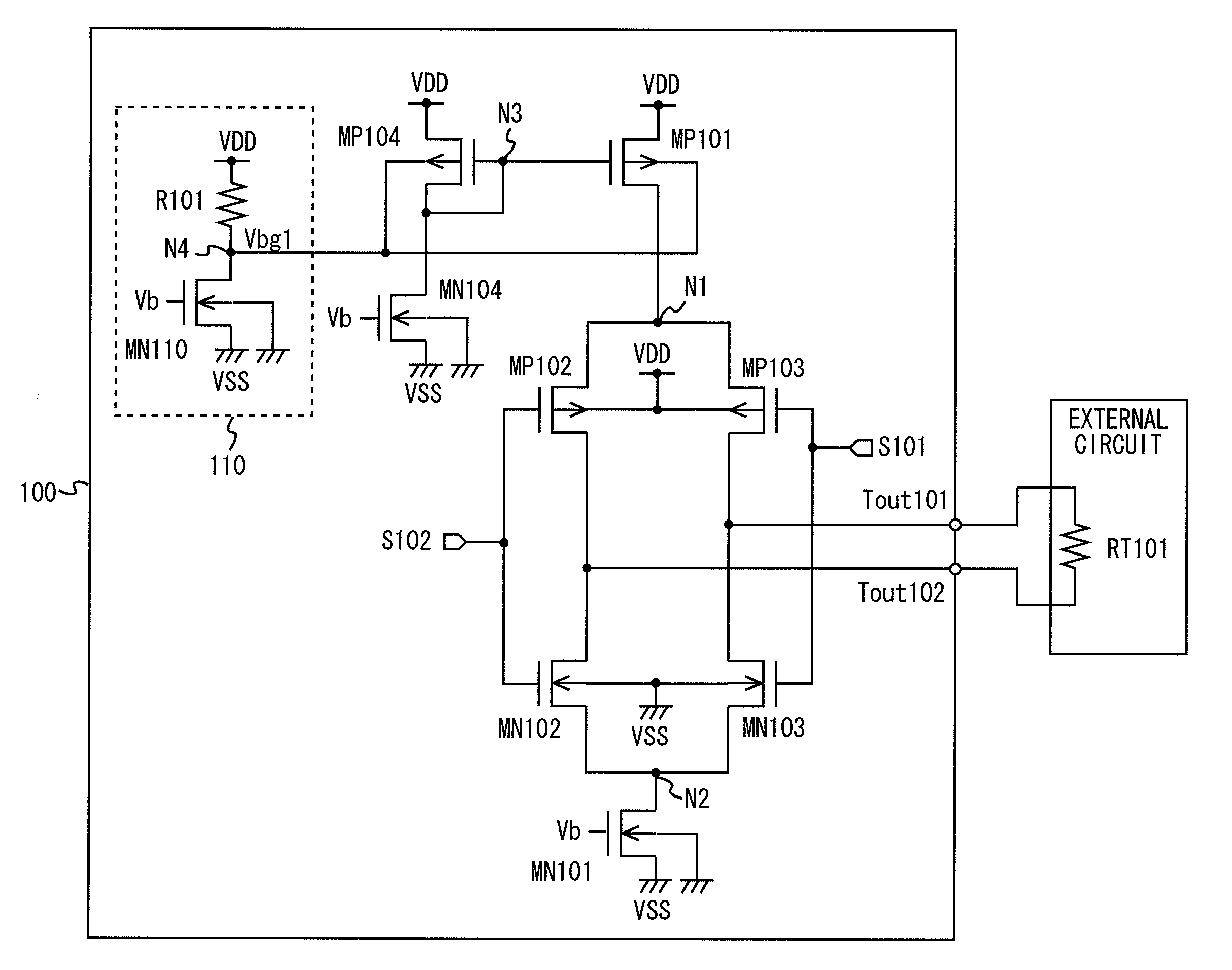
[0033]Now, a first embodiment of the present invention will be described in detail with reference to the accompanying drawings. The first embodiment is formed by applying the present invention to a drive circuit employing LVDS (hereafter referred to as an “LVDS drive circuit”). FIG. 1 shows the configuration of an LVDS drive circuit 100 according to the first embodiment.
[0034]As shown in FIG. 1, the LVDS drive circuit 100 includes PMOS transistors MP101 to MP104, NMOS transistors MN101 to MN104, and a bias voltage generation unit 110.
[0035]For the PMOS transistor MP101, its source is connected to a power supply voltage terminal VDD, its drain to a node N1, and its gate to a node N3. For the PMOS transistor MP104, its source is connected to a power supply voltage terminal VDD, and its drain and gate to the node N3. For the NMOS transistor MN104, its drain is connected to the node N3, and its source to a ground voltage terminal VSS. A predetermined bias voltage Vb is applied to the ga...
second embodiment
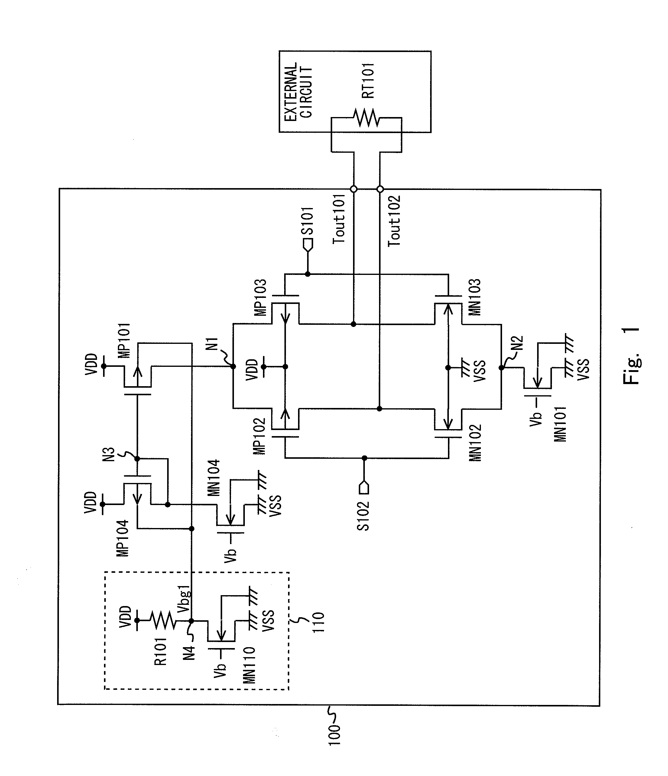
[0050]Now, a second embodiment of the present invention will be described in detail with reference to the accompanying drawings. As with the first embodiment, the second embodiment is formed by applying the present invention to an LVDS drive circuit. FIG. 2 shows the configuration of an LVDS drive circuit 200 according to the second embodiment.
[0051]As shown in FIG. 2, the LVDS drive circuit 200 includes PMOS transistors MP101, MP104, MP102, and MP103, NMOS transistors MN101 to MN104, and a bias voltage generation unit 210. Of the reference numerals shown in FIG. 2, the elements given the same reference numerals as those shown in FIG. 1 represent elements identical or similar to those shown in FIG. 1.
[0052]The differences between the second and first embodiments are the back gate potential of the PMOS transistors MP102 and MP103 and the bias voltage generation unit 210. These differences will be focused on in the following description and the same elements as those in the first embo...
third embodiment
[0072]Now, a third embodiment of the present invention will be described in detail with reference to the accompanying drawings. As with the second embodiment, the third embodiment is formed by applying the present invention to an LVDS drive circuit. FIG. 4 shows the configuration of an LVDS drive circuit 300 according to the third embodiment.
[0073]As shown in FIG. 4, the LVDS drive circuit 300 includes PMOS transistors MP101, MP104, MP102, MP103, and MP301, NMOS transistors MN102 to MN104, and a bias voltage generation unit 310. Of the reference numerals shown in FIG. 4, the elements given the same reference numerals as those shown in FIG. 2 represent elements identical or similar to those shown in FIG. 2.
[0074]The differences between the third and second embodiments are the PMOS transistor MP301 and the bias voltage generation unit 310. The differences will be focused on in the following description and the same elements as those in the second embodiment will not be described.
[0075...
PUM
 Abstract
Description
Claims
Application Information
 - R&D Engineer
- R&D Manager
- IP Professional
- Industry Leading Data Capabilities
- Powerful AI technology
- Patent DNA Extraction
Browse by: Latest US Patents, China's latest patents, Technical Efficacy Thesaurus, Application Domain, Technology Topic.
© 2024 PatSnap. All rights reserved.Legal|Privacy policy|Modern Slavery Act Transparency Statement|Sitemap