Methods and Systems for Surface Enhanced Optical Detection

a technology of enhanced optical detection and surface, applied in the field of sensing, can solve the problems of limiting the molecular binding to the electric field enhanced region in the sers application, the enhancement factor is still not high enough, and the total interaction volume between radiation and molecules is limited. to achieve the effect of high electromagnetic field enhancement factor

Inactive Publication Date: 2013-01-03
INTERUNIVERSITAIR MICRO ELECTRONICS CENT (IMEC VZW) +2
View PDF16 Cites 23 Cited by
  • Summary
  • Abstract
  • Description
  • Claims
  • Application Information

AI Technical Summary

Benefits of technology

[0006]It is an object of embodiments of the present invention to provide good surface enhanced optical detection substrates for sensing purposes, as well as methods of manufacturing them and methods and systems of using such substrates. It is an advantage of at least some embodiments according to the present invention that a high electromagnetic field enhancement factor can be reached, i.e. sufficiently high for most applications envisaged.
[0007]It is an advantage of at least some embodiments according to the present invention that the integrated enhancement factor can be good, i.e. that a good enhancement factor can be reached for a significant large interaction volume between the radiation and the substances to be measured.
[0008]It is an advantage of at least some embodiments according to the present invention that substrates with the above mentioned good enhancement factor and / or the above mentioned good integrated enhancement factor can be obtained in a reproducible way.

Problems solved by technology

By these methods, the reduced-symmetrical structures of nanoshells, such as nano aperture or nanotip, are usually oriented randomly or with their aperture downward, which obviously limits the molecular binding to the electric field enhanced regions in SERS applications.
Nevertheless, for a significant number of applications, the enhancement factor still is not high enough.
For the nanorings, the positions where high electric fields are reached are limited to the top edges of the nanorings, thus limiting the total interaction volume between the radiation and the molecules and thus limiting the integrated enhancement factor.

Method used


Image

  • Methods and Systems for Surface Enhanced Optical Detection
  • Methods and Systems for Surface Enhanced Optical Detection
  • Methods and Systems for Surface Enhanced Optical Detection

Examples


Embodiment Construction

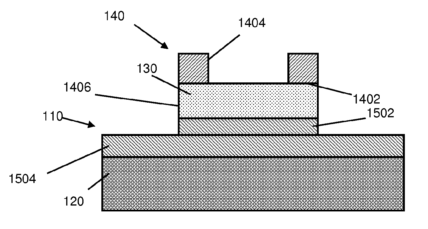
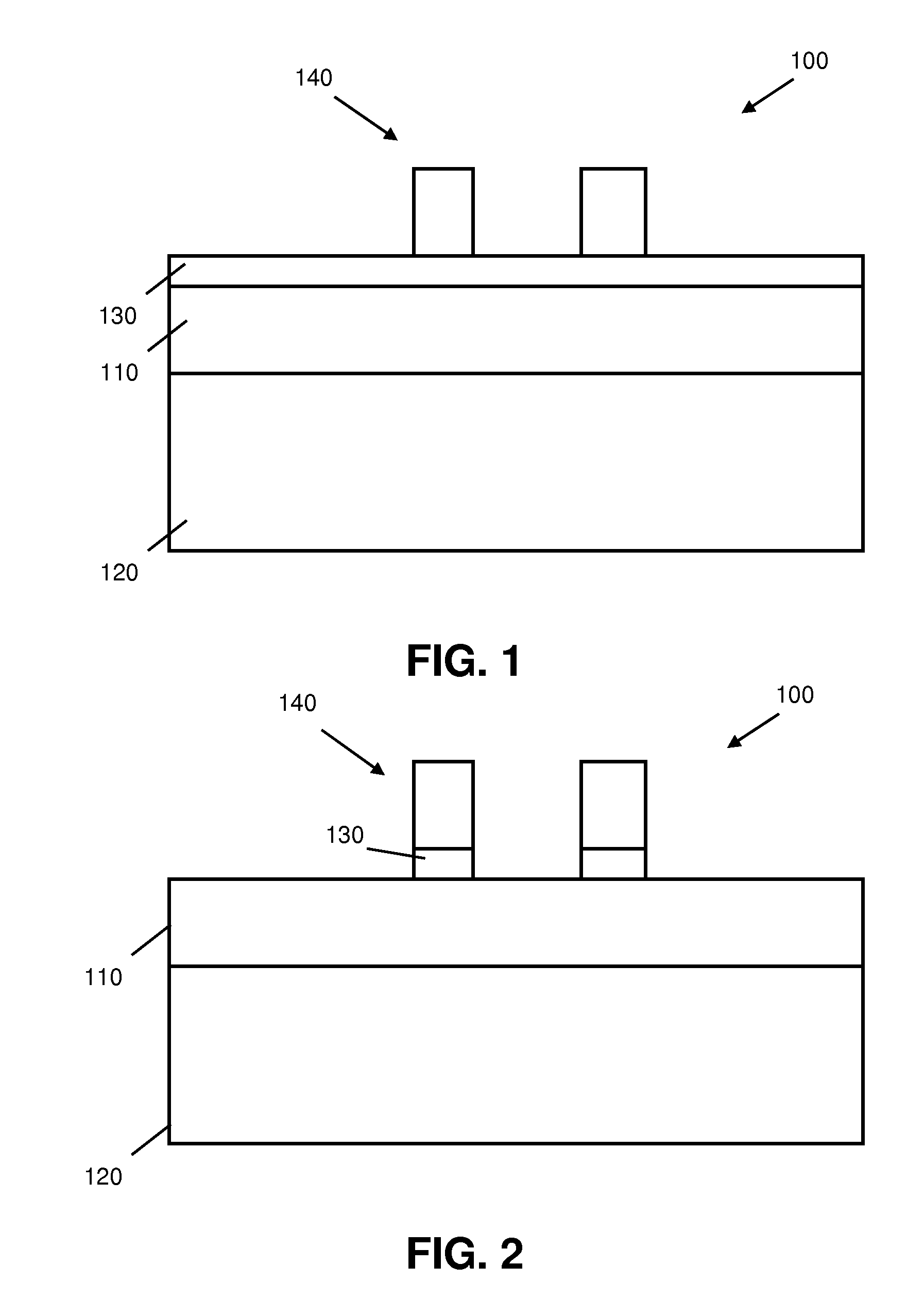
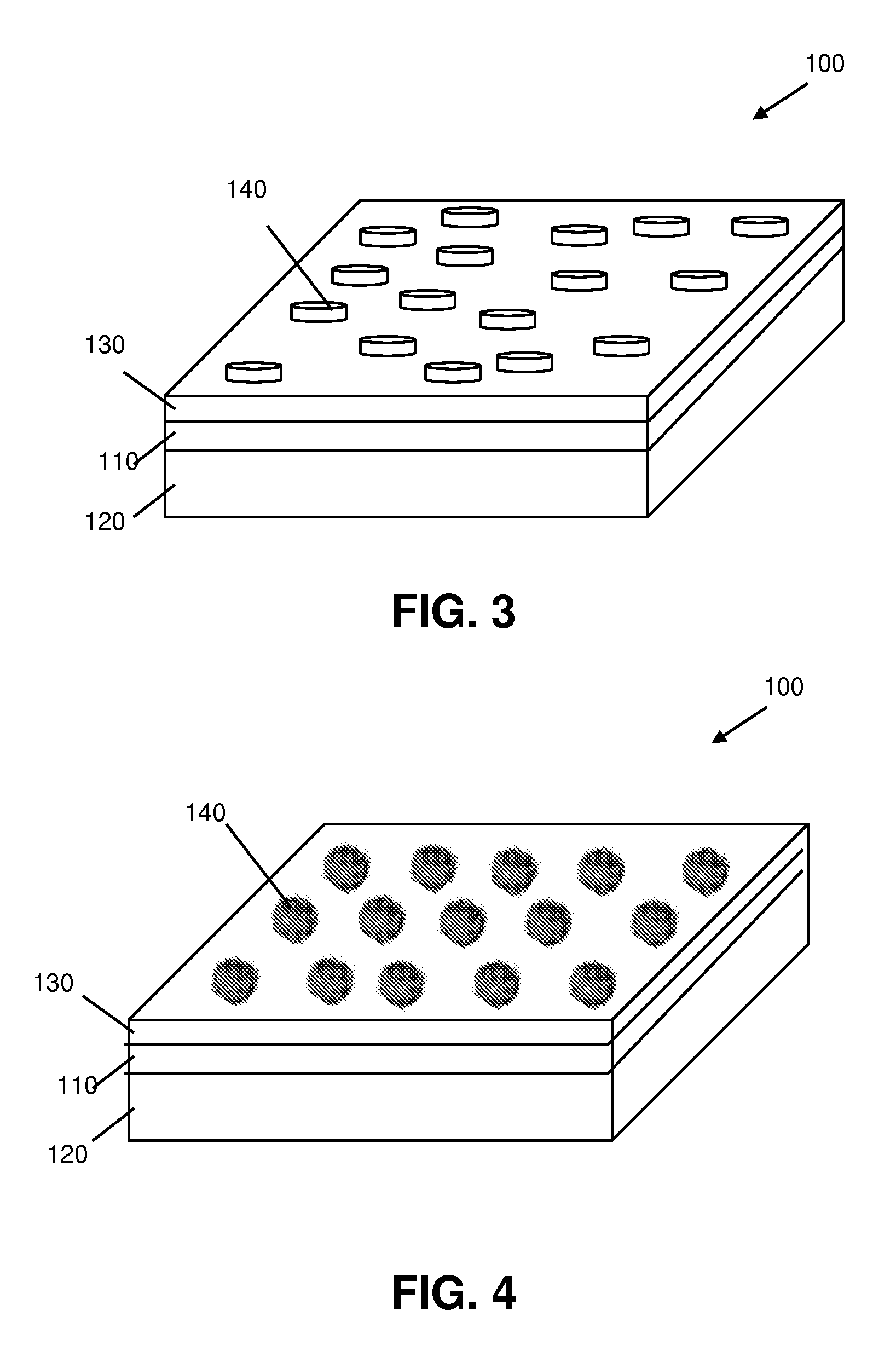
[0070]Where in embodiments of the present invention reference is made to “nanoparticle” reference is made to all types of nanoparticles such as for example open nanoparticles, spherical nanoparticles, nanodisks, etc.

[0071]Where in embodiments of the present invention reference is made to nano features, reference is made to nanopores, nano holes, nanoparticles, etc.

[0072]As used herein and unless stated otherwise, the term “open nanoparticles” relates to a nano particle being a nanoring or an open nanoshell or open shell nanoparticle. An open nanoshell or open shell nanoparticle refers to a nanoparticle with a dielectric core and non-complete or partial electrically conductive layer around the core. A nanoring or nanoring particle is a nanostructure having a ring or toroidal shape. An open nanoshell may be a non-spherical symmetrical portion of a nanosphere.

[0073]As used herein and unless stated otherwise, the term “nano” is used for referring to objects having typical characteristic...


PUM

PropertyMeasurementUnit
lengthsaaaaaaaaaa
lengthsaaaaaaaaaa
lengthsaaaaaaaaaa

Abstract

A substrate is described that is suitable for surface enhanced optical detection. The substrate comprises an electrically conductive layer (110), such as for example a gold layer. It furthermore comprises at least one nanoparticle (1404) comprising an electrically conductive portion. The electrically conductive portion in some embodiments provides an opening to an underlying material. Such at least one nanoparticles (1404) thus may for example be a nanoring, a nanodisc, or a non-spherical nanoshell. The substrate furthermore comprises a dielectric spacer (1406) for spacing the electrically conductive layer from the at least one nanoparticles. The dielectric spacer (1406) is a dielectric material substantially only present under the at least one nanoparticle (1404), leaving the electrically conductive layer (110) uncovered from dielectric material at positions away from the nanoparticles (1404). The at least one nanoparticle (1404) and the dielectric spacer (1406) are interfaced along a first major surface (1402) and the at least one nanoparticle (1404) comprises an upstanding surface not in line with an upstanding surface of the dielectric spacer (1406).

Description

FIELD OF THE INVENTION[0001]The invention relates to the field of sensing. More particularly, the present invention relates to substrates for sensing via surface enhanced optical detection, methods of manufacturing them and methods and systems of using such substrates.BACKGROUND OF THE INVENTION[0002]Gold (Au) nano shells are nanoparticles usually composed of a dielectric core, typically silica, coated with an ultrathin Au layer. These nanoparticles show interesting optical and chemical properties for the applications of surface-enhanced Raman spectroscopy (SERS) sensor, surface plasmon resonance (SPR) sensor, drug delivery, biomedical imaging and cancer therapeutics among others.[0003]Reducing symmetry of Au nanoshells geometry shows interesting properties. It is possible to excite different plasmon modes in these particles when compared to standard particles. These particles show angle dependent plasmon resonance. This unique property may lead to a new class of optically active na...

Claims


Application Information

Patent Timeline
Patent Type & Authority Applications(United States)
IPC IPC(8): G01J3/44B32B5/16B05D5/12B05D3/10B82Y30/00
CPCB82Y15/00G01N21/553G01N21/554G01N21/648Y10T428/25B82Y30/00B22F2001/0029Y10S977/773G01N21/658
Inventor VAN DORPE, POLLODEWIJKS, KRISTOFSHIOI, MASAHIKOYE, JIAN
Owner INTERUNIVERSITAIR MICRO ELECTRONICS CENT (IMEC VZW)
Why Eureka
Try Eureka