Light emitting device

a technology of light emitting devices and side views, which is applied in the direction of solid-state devices, lighting and heating devices, lighting support devices, etc., can solve the problems of reducing reliability, affecting the effort to form a thinner and smaller light emitting device, and uneven stress distribution, so as to prevent the breakage of bonding wires and improve reliability.

Inactive Publication Date: 2013-01-03
TOYODA GOSEI CO LTD
View PDF7 Cites 1 Cited by
  • Summary
  • Abstract
  • Description
  • Claims
  • Application Information

AI Technical Summary

Benefits of technology

[0024]Consequently, according to the first aspect, the heat generated from the individual light emitting elements can escape to the outer side by conducting through various different heat dissipation routes via individual lead frames. It is possible to improve the heat dissipation property, as the heat dissipation routes are divided from each other.
[0037]As a result, according to the sixth aspect, the bonding wires where a high current flows are protected by the accommodating recession and the column-shaped parts, so that it is possible to prevent wire breakage of the bonding wires, and hence it is possible to further improve reliability.

Problems solved by technology

However, the invention described in Patent Reference 1 has the following problem: because the dimensions and shapes of the individual lead frames as well as their arrangements are asymmetric respect to the case, heat is deviated in the light emitting device so that localized high temperature portions are generated, and, the stress distribution becomes uneven due to the thermal expansion applied on the case.
Consequently, various troubles take place, such as separation of the lead frames buried in the case from the case, separation of the sealing resin filled in the case from the case, separation of the lead frame and the sealing resin from each other, breaking of bonding wires connecting the light emitting elements, etc., resulting in decreasing reliability, which is undesirable.
However, when the invention of Patent Reference 2 is adopted in a side view-type light emitting device, in order to enable escape of the heat of the base arranged at the center to the outer side, it is necessary to connect a hanger lead or other heat dissipation dedicated lead frame protruding to the outer side to the base, yet the heat dissipation dedicated lead frame protruding to the outer side hampers the effort to form a thinner and smaller light emitting device, which is undesirable.
In addition, as a plurality of light emitting elements is mounted on the base arranged at the center, the heat dissipation route cannot be divided, and the heat dissipation property is hampered, which is undesirable, too.

Method used


Image

  • Light emitting device
  • Light emitting device
  • Light emitting device

Examples


embodiment 1

Operation and Advantages of Embodiment 1

[0073]The operation and advantages of the light emitting device 10 in Embodiment 1 are as follows.

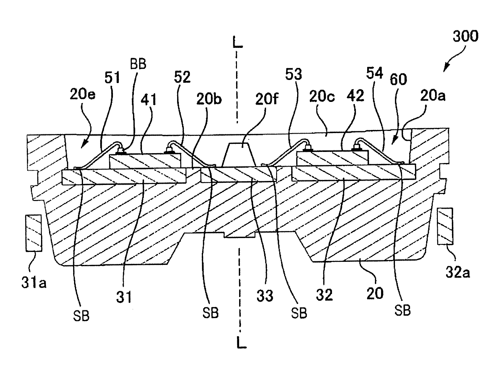
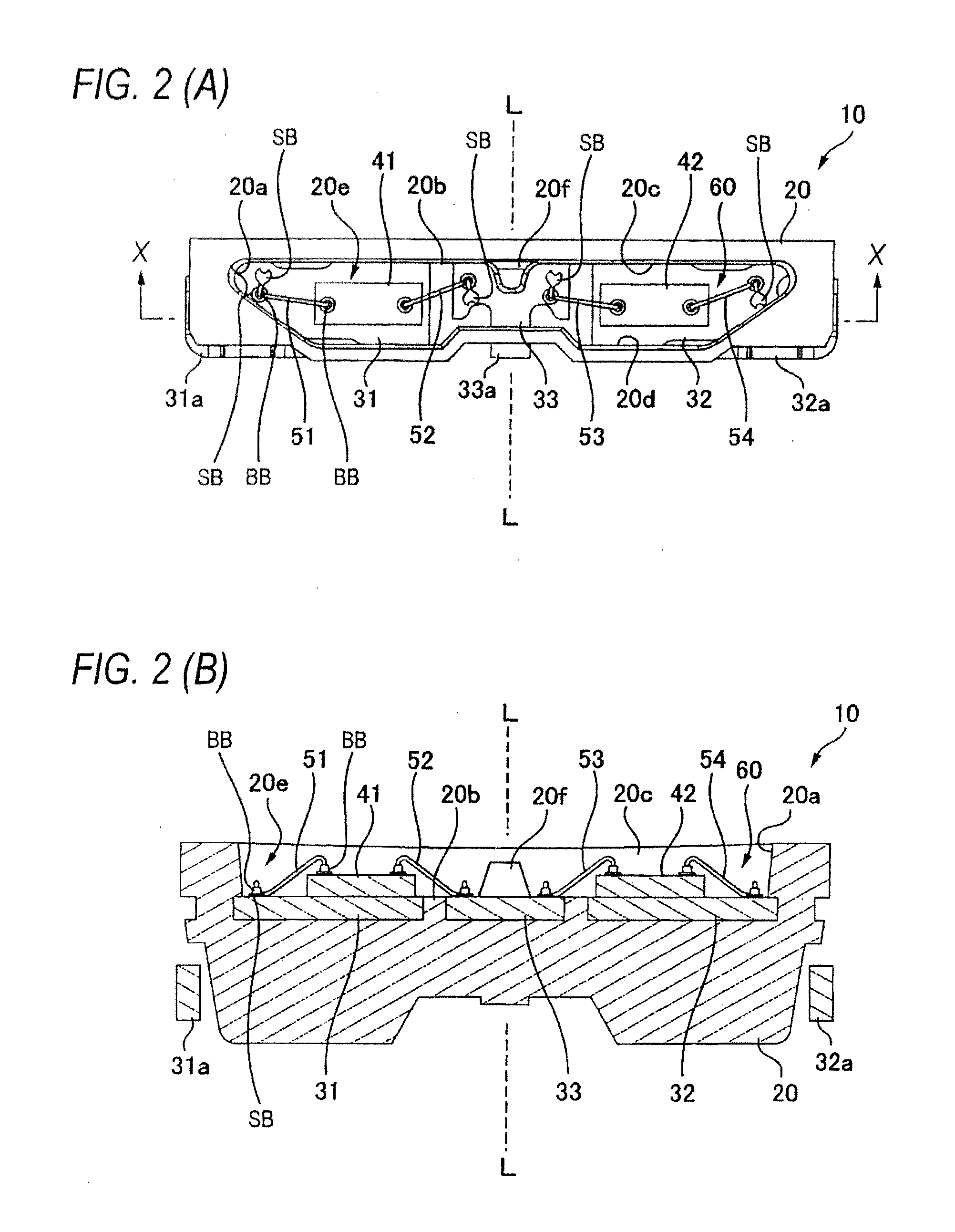
[0074](1) The lead frames 31 to 33 are arranged side-by-side in the longitudinal direction of the case 20 and are buried there. The outer surfaces of the lead frames 31 to 33 are exposed from the bottom surface of the accommodating recession 20e, and the outer surfaces of the lead frames 31 to 33 are formed flush with the bottom surface of the accommodating recession 20e, and the surfaces of the lead frames 31 to 33 are arranged coplanar with each other.

[0075]The light emitting elements 41, 42 are carried in the lead frames 31, 32 arranged in the two end portions in the longitudinal direction of the case 20. The lead frames 31 to 33, the case 20 and the light emitting elements 41, 42 are formed in a linear symmetric configuration with respect to the central line L that bisects the longitudinal direction of the light emitting device 10.

[0076]In oth...

second embodiment

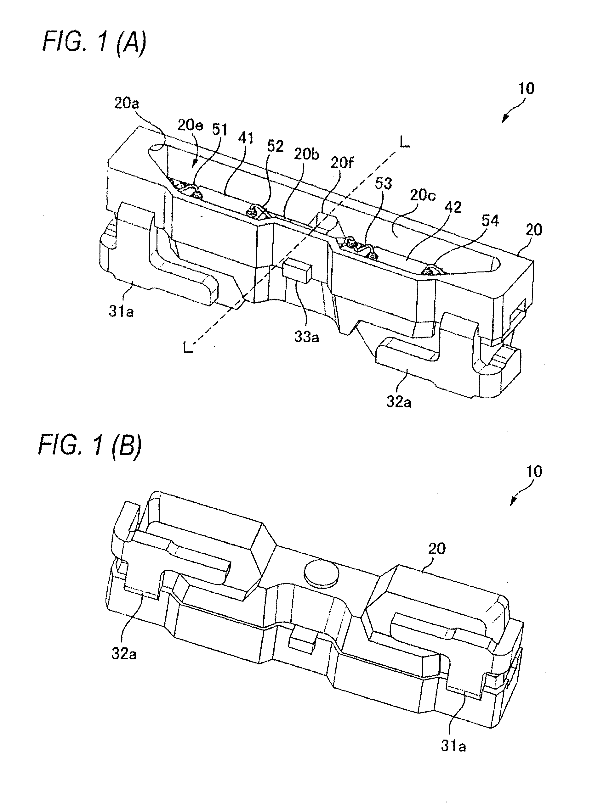
[0090]As shown in FIG. 3, the light emitting device 100 of Embodiment 2 is a side view-type light emitting device including the case 20 (opening portion 20a, bottom surface 20b, inner side surfaces 20c, 20d, accommodating recession 20e, and column-shaped part 20f), lead frames 31 to 33, light emitting elements 41, 42, bonding wires 51 to 54, sealing resin 60, etc.

[0091]The case 20 in Embodiment 2 is the same as the case 20 in Embodiment 1. Consequently, the oblique view of the light emitting device 100 is similar to the light emitting device 10 in Embodiment 1 as shown in FIG. 1.

[0092]Embodiment 2 differs from Embodiment 1 in that the light emitting elements 41, 42 are not arranged in a linear asymmetric configuration with reference to the central line L, and the distance from the light emitting device 41 to the inner side surface 20c of the case 20 is shorter than the distance from the light emitting device 42 and the inner side surface 20c.

[0093]That is, in Embodiment 2, the ligh...

embodiment 3

[0099]As shown in FIG. 4, the light emitting device 200 of Embodiment 3 is a side view-type light emitting device including a case 20 (opening portion 20a, bottom surface 20b, inner side surfaces 20c, 20d, accommodating recession 20e, and column-shaped part 20f), lead frames 31 to 33, light emitting elements 41, 42, bonding wires 51, 54, 201, sealing resin 60, etc.

[0100]In Embodiment 3, the case 20 is the same as the case 20 of Embodiment 1. Consequently, the oblique view of the light emitting device 200 is nearly the same as the light emitting device 10 in Embodiment 1 shown in FIG. 1.

[0101]Embodiment 3 differs from Embodiment 1 in the following features.

[0102][a] It does not have the lead frame 33 and the bonding wires 52, 53.

[0103][b] The light emitting elements 41, 42 are directly connected with the bonding wire 201 without via lead frames.

[0104][c] It does not have the column-shaped part 20f.

[0105]Consequently, Embodiment 3 can also have the same operation and advantages as th...


PUM


Abstract

A light emitting device comprises two or more light emitting elements, two or more lead frames electrically connected to the light emitting elements, and a case formed as a slender flat box shape and having an accommodating recession for accommodating the light emitting elements and the lead frame, wherein the lead frames are buried in the case and provided side by side in a longitudinal direction of the case, and the surfaces of the lead frames are arranged coplanar, the light emitting elements are mounted on the lead frames, and the plurality of lead frames and the case are arranged in a nearly linear symmetric configuration with respect to a central line that bisects the light emitting device in the longitudinal direction, so that no uneven heat distribution takes place.

Description

BACKGROUND OF THE INVENTION[0001]1. Field of the Invention[0002]The present invention relates to a side view-type light emitting device.[0003]2. Description of the Related Art[0004]Patent Reference 1 shows a side view-type light emitting device (side surface light emitting device) as the thin-type light emitting device adopted in the backlight of liquid crystal display.[0005]In addition, Patent Reference 2 describes a light emitting device comprising a plurality of light emitting elements, a first resin molding that carries the light emitting elements, and a second resin molding that covers the light emitting elements.[0006]Patent Reference 1: Japanese Patent No. 4239509[0007]Patent Reference 2: JP-A-2008-300694[0008]According to the invention described in Patent Reference 1, a plurality of light emitting elements are arranged side-by-side on the same line in the longitudinal direction of the case (package); individual light emitting elements are mounted on the individual lead frame...

Claims


Application Information

Patent Timeline
Patent Type & Authority Applications(United States)
IPC IPC(8): F21V21/00
CPCH01L24/48H01L25/0753H01L33/486H01L33/62H01L2224/48247H01L2224/48465H01L2224/48997H01L2224/48091H01L2924/00014H01L2924/00H01L2224/48455H01L2224/85951H01L2924/19107H01L2924/181H01L2224/45099H01L2224/05599H01L33/48
Inventor KOKUBU, HIDEKIFUKUI, KOSEIHAYASHI, TOSHIMASADEMUKAI, YUKIHIRO
Owner TOYODA GOSEI CO LTD
Why Eureka
Try Eureka