Wafer Inspection

a wafer and inspection system technology, applied in the direction of luminescent dosimeters, optical radiation measurement, instruments, etc., can solve the problems of limiting the reach of throughput, undetectable alteration of sample properties, and limited spot inspection systems

Active Publication Date: 2013-01-17
KLA CORP
View PDF24 Cites 148 Cited by
  • Summary
  • Abstract
  • Description
  • Claims
  • Application Information

AI Technical Summary

Problems solved by technology

However, as the dimensions of semiconductor devices decrease, inspection becomes even more important to the successful manufacture of acceptable semiconductor devices because smaller defects can cause the devices to fail.
Furthermore, spot-illuminated inspection systems are practically limited to dozens of spots due to the complexities of illumination optics and of integrating individual sensors thereby limiting achievable throughput.
One further disadvantage of spot and line scanning systems is the illumination energy is concentrated in relatively small areas, increasing the power density on the inspected surface, which can undesirably alter the sample properties.
Despite the advantage of area inspection systems, as described above and in the art (e.g., U.S. Pat. No. 7,286,697 to Guetta), implementation of this configuration on an R-Theta platform has proven challenging, as there is an inherent mismatch of the spiral sequence of generated images with the rectilinear nature of most two-dimensional array sensors.
Detection of defects by the aligning and registration of polar images in real time is a computationally intensive activity.
Furthermore, the additional noise added to the measurement by most two-dimensional silicon-based sensors, as compared to discrete detectors such as photomultiplier tubes (PMTs), has in practice reduced the sensitivity performance of such systems.
On XY-based area inspection systems, the coordinate mismatch problem does not exist, but previous embodiments of such systems have not been able detect all defects of interest at high speeds due to lack of flexibility of the illumination and collection subsystems.

Method used


Image

  • Wafer Inspection
  • Wafer Inspection
  • Wafer Inspection

Examples


Embodiment Construction

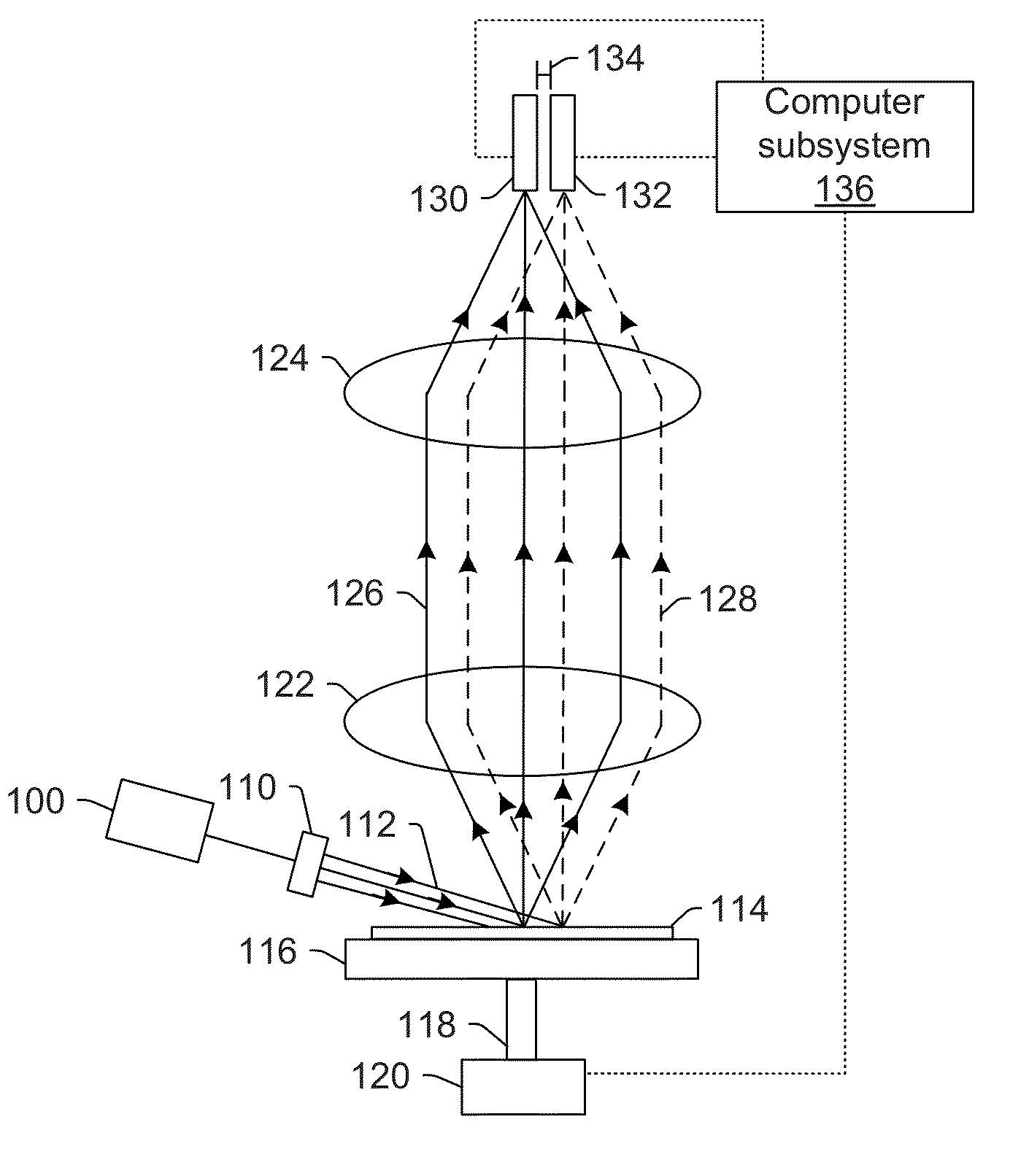
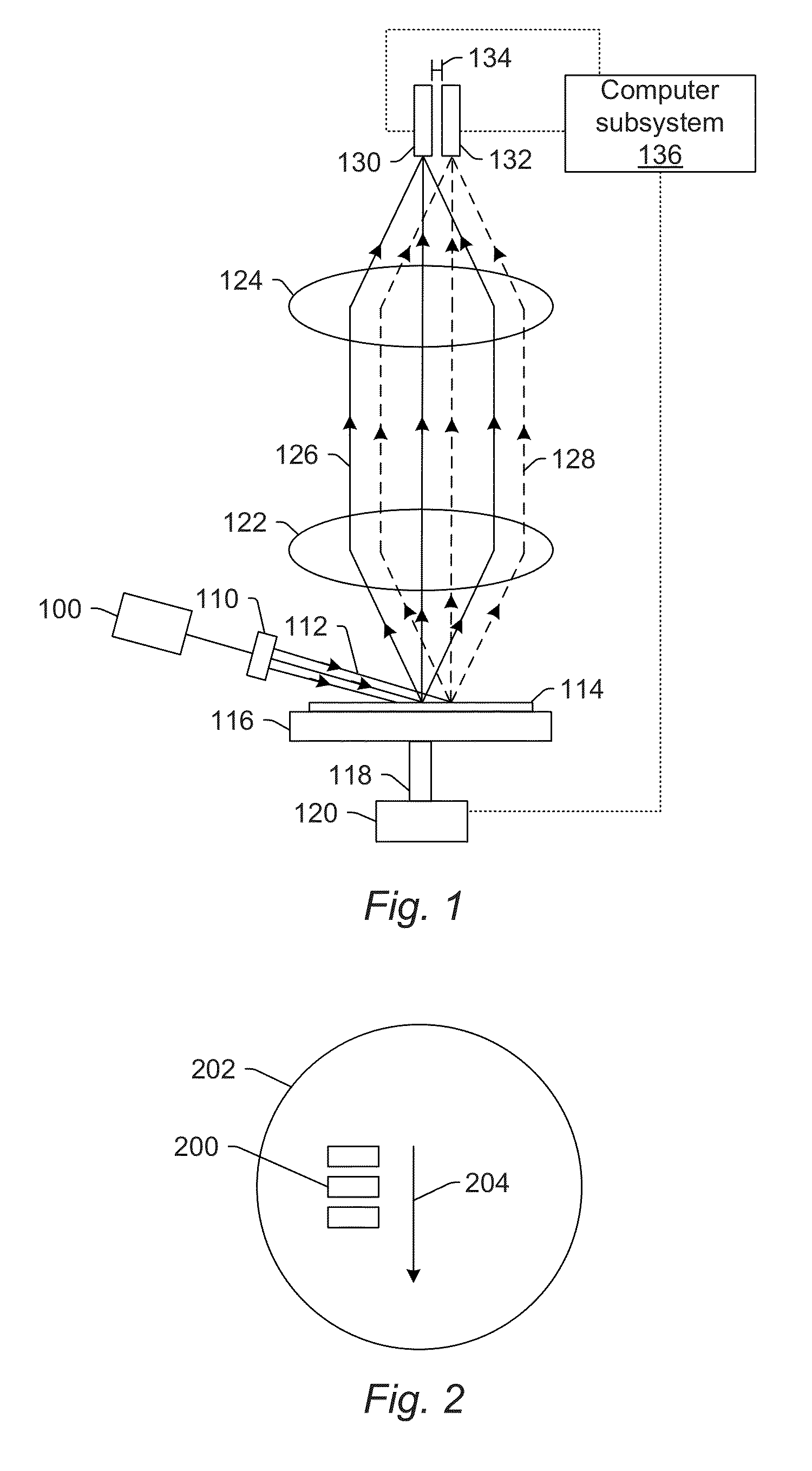
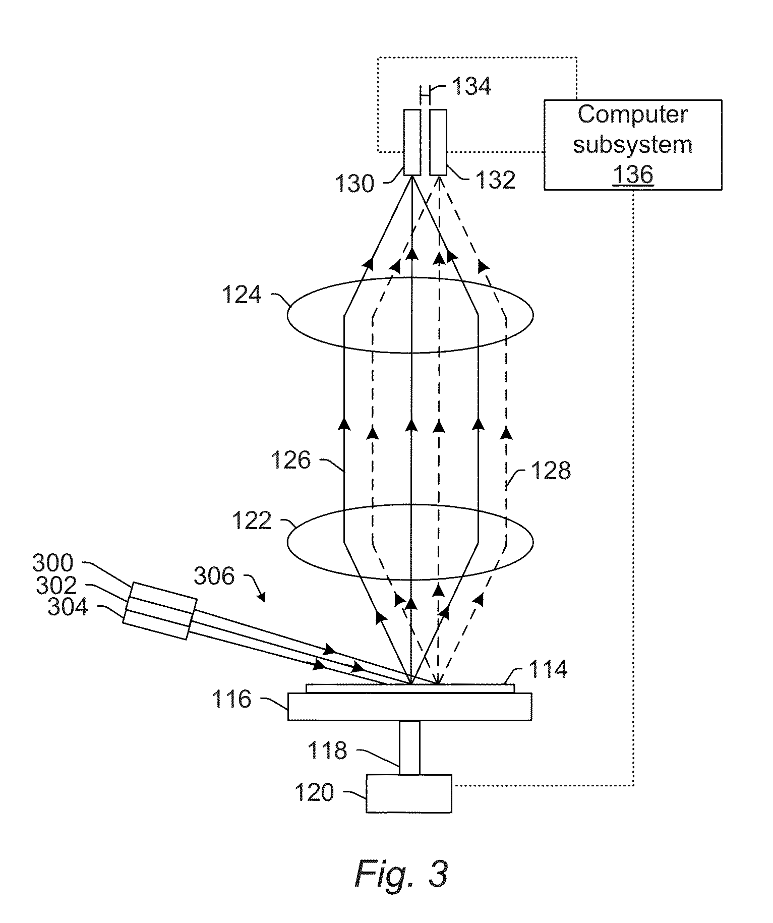
[0033]In general, the embodiments described herein relate to wafer inspection methods and systems that include the following: illumination (e.g., laser illumination) is incident on the wafer; the wafer or illumination spot(s) on the wafer is / are translated in some fashion; scattered light is collected by a collection subsystem (which may include a collection objective); in the collection optics, the scattered light may be divided based on selectable polarization and / or scattering angle characteristics; selected portion(s) of the scattered light are directed onto one or more sensors; and defects are detected by processing output (e.g., image information) generated by the sensor(s).

[0034]Turning now to the drawings, it is noted that the figures are not drawn to scale. In particular, the scale of some of the elements of the figures is greatly exaggerated to emphasize characteristics of the elements. It is also noted that the figures are not drawn to the same scale. Elements shown in mo...


PUM

PropertyMeasurementUnit
oblique angleaaaaaaaaaa
diameteraaaaaaaaaa
diameteraaaaaaaaaa

Abstract

Systems configured to inspect a wafer are provided.

Description

CROSS-REFERENCE TO RELATED APPLICATIONS[0001]This application claims priority to U.S. Provisional Application No. 61 / 506,892 entitled “Sample Inspection System,” filed Jul. 12, 2011, which is incorporated by reference as if fully set forth herein.BACKGROUND OF THE INVENTION[0002]1. Field of the Invention[0003]This invention generally relates to systems configured to inspect a wafer.[0004]2. Description of the Related Art[0005]The following description and examples are not admitted to be prior art by virtue of their inclusion in this section.[0006]Inspection processes are used at various steps during a semiconductor manufacturing process to detect defects on wafers to promote higher yield in the manufacturing process and thus higher profits. Inspection has always been an important part of fabricating semiconductor devices. However, as the dimensions of semiconductor devices decrease, inspection becomes even more important to the successful manufacture of acceptable semiconductor devi...

Claims


Application Information

Patent Timeline
Patent Type & Authority Applications(United States)
IPC IPC(8): G01N21/956
CPCG01N21/9501G01N21/956G01N21/47H01L22/12H01L21/67242H01L22/30G01N21/8806G01N21/8851
Inventor ROMANOVSKY, ANATOLYMALEEV, IVANKAVALDJIEV, DANIELYUDITSKY, YURYWOLL, DIRKBIELLAK, STEPHEN
Owner KLA CORP
Why Eureka
Try Eureka