Integrated circuit comprising at least an integrated antenna

a technology of integrated circuits and antennas, applied in the direction of electronic circuit testing, inductance, instruments, etc., can solve the problems of reducing the efficiency of the antenna, and the embedded type of the antenna, and reducing the quality factor q. , to achieve the effect of reducing the cost of antennas, and reducing the efficiency of antennas

Active Publication Date: 2013-01-31
STMICROELECTRONICS SRL
View PDF10 Cites 39 Cited by
  • Summary
  • Abstract
  • Description
  • Claims
  • Application Information

AI Technical Summary

Benefits of technology

[0095]The problem is solved also by a testing system of at least one integrated circuit provided with an antenna and realized as above indicated, the testing system comprising an antenna card directly as...

Problems solved by technology

The drawback of these currents is thus that they produce a magnetic flow that opposes against the variation of magnetic flow produced by the antenna and/or by the inducer present in the chip with a consequent reduction of its efficiency, in particular the negative mutual coupling of the currents reduces the value of the effective inductance, while the energy dissipated by the eddy currents reduces the quality factor Q, as it is evident from the following relation (referred to an inducer under optimal conditions):
In each case, the antennas of the embedded type, now very used for RFId or...

Method used


Image

  • Integrated circuit comprising at least an integrated antenna
  • Integrated circuit comprising at least an integrated antenna
  • Integrated circuit comprising at least an integrated antenna

Examples


first embodiment

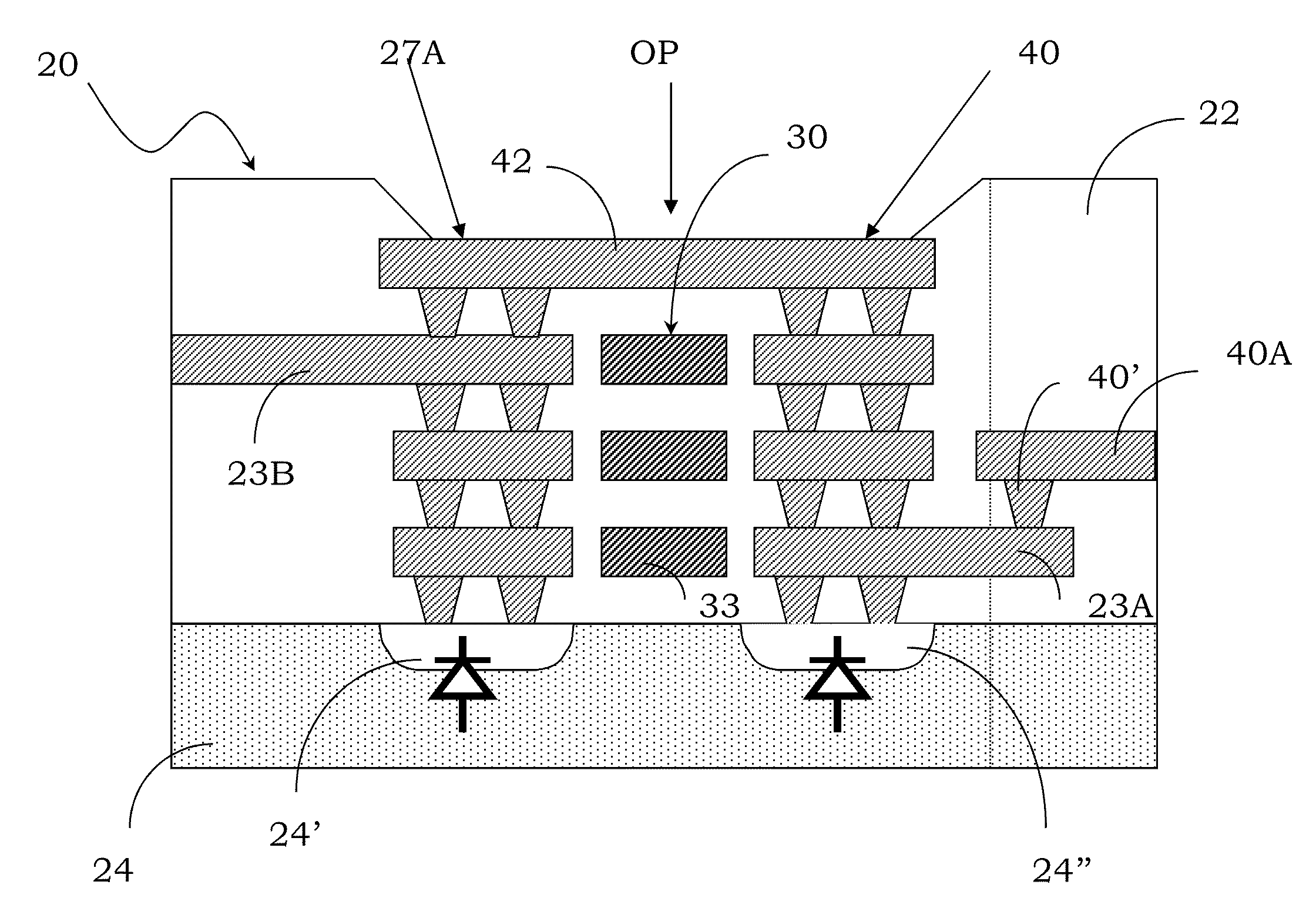
[0134]In particular, in a first embodiment shown in FIG. 5B, the first conductive lines 33 belonging to each plane form a coil of the integrated antenna 30. A coil is connected to another one by means of conductive connections, for example metallic vias, arranged perpendicularly to the coil itself for connecting conductive lines 33 belonging to different planes.

[0135]According to this aspect, the antenna 30 develops then in the vertical direction, starting from the substrate 24 and inside the peripheral portion 21 of the integrated circuit 20 close to the scribe line 22.

[0136]It is to be noted that the antenna 30, positioned in correspondence with the peripheral portion 21 of the integrated circuit 20, where the seal ring 25 is already usually realized, does not introduce problems regarding the routing of the internal signals of the integrated circuit 20 itself, a suitable routing configuration being already provided given the presence of the seal ring itself.

[0137]Moreover, thanks ...

second embodiment

[0184]A second embodiment is schematically shown with reference to FIG. 19.

[0185]In particular, the integrated circuit 20 comprises at least one first plurality of conductive lines 51 that surround its active area 20A in its peripheral portion 21 in correspondence with the scribe line 22 and realize the antenna 30, as well as a second plurality of conductive lines 52, still realized in its peripheral portion 21 so as to surround its active area 20A form the seal ring 25. Also in this case, as seen for the previous embodiment, the conductive lines belonging to different planes are suitably connected by means of conductive connections, the seal ring 25 and the antenna 30 having a vertical development in the scribe line 22 starting from the substrate 24 of the integrated circuit 20 itself, as previously seen.

[0186]More in particular, the first plurality of conductive lines 51 is interrupted in correspondence with a first cutting area, indicated with C1 in the figure, each conductive li...

third embodiment

[0200]In a third embodiment, shown schematically in FIG. 25, in the peripheral portion 21 of the integrated circuit 20 adjacent to the scribe line 22 at least one conductive line 33 is realized, that forms the antenna 30. According to this embodiment, a trench structure 60 is suitably realized in a central portion 22A of the scribe line 22 that separates a first and a second integrated circuit 20 and 20′, as schematically shown in FIG. 26A. In this case, as it will be better clarified hereafter in the description, the integrated circuit 20 does not comprise any seal ring.

[0201]In fact, the trench structure 60 is realized so as to penetrate at least into the depth of the substrate 24, creating a housing area of the cutting tools for the singulation of the integrated circuits 20, this singulation interesting only the substrate 24 and thus not requesting the presence of a seal ring to protect the integrated circuit 20. Moreover, the singulation operation does not risk in this way to da...


PUM


Abstract

An integrated circuit on a substrate including at least one peripheral portion that surrounds an active area and is realized close to at least one scribe line providing separation with other integrated circuits realized on a same wafer. The integrated circuit includes at least one conductive structure that extends in its peripheral portion on different planes starting from the substrate and realizes an integrated antenna for the circuit.

Description

CROSS REFERENCE TO RELATED APPLICATIONS[0001]This application claims the priority benefit of Italian patent application number MI2011A001416, filed on Jul. 28, 2011, entitled PERIPHERAL ANTENNA, which is hereby incorporated by reference to the maximum extent allowable by law.BACKGROUND[0002]1. Technical Field[0003]Embodiments relate to an integrated circuit provided with at least one integrated antenna. Embodiments particularly, but not exclusively, relate to an wafer integrated circuit and the following description is made with reference to this field of application by way of illustration only.[0004]2. Discussion of the Related Art[0005]As it is well known, for the electric selection of devices executed on wafer, i.e. the so called testing EWS (acronym from “Electrical-Wafer-Sorting”), it is necessary to electrically connect a tester or ATE (acronym from “Automated Test Equipment”) that executes measures on a wafer whereon there are electronic components to be tested or selected or...

Claims


Application Information

Patent Timeline
IPC IPC(8): G01R1/00H01L29/02
CPCG01R31/2889H01L2224/05553H01L22/32H01L22/34G01R31/3025H01L2224/02166H01L2224/0401H01L2924/15311H01L2224/48465H01L2224/48091H01L2224/16225H01L2924/30107H01L2924/00014H01L2924/00H01L2224/04042H01L2924/181H01L28/10H01L2924/00012H01L23/528H01L23/564H01L23/585H01L23/66H01L24/05H01L29/0642H01L2223/6677H01L23/544H01L25/0657G01R31/2834
Inventor PAGANI, ALBERTOFINOCCHIARO, ALESSANDRO
Owner STMICROELECTRONICS SRL
Why Eureka
Try Eureka