Three-dimensional integrated circuit, processor, semiconductor chip, and manufacturing method of three-dimensional integrated circuit
- Summary
- Abstract
- Description
- Claims
- Application Information
AI Technical Summary
Benefits of technology
Problems solved by technology
Method used
Image


Examples
embodiment
1. Embodiment
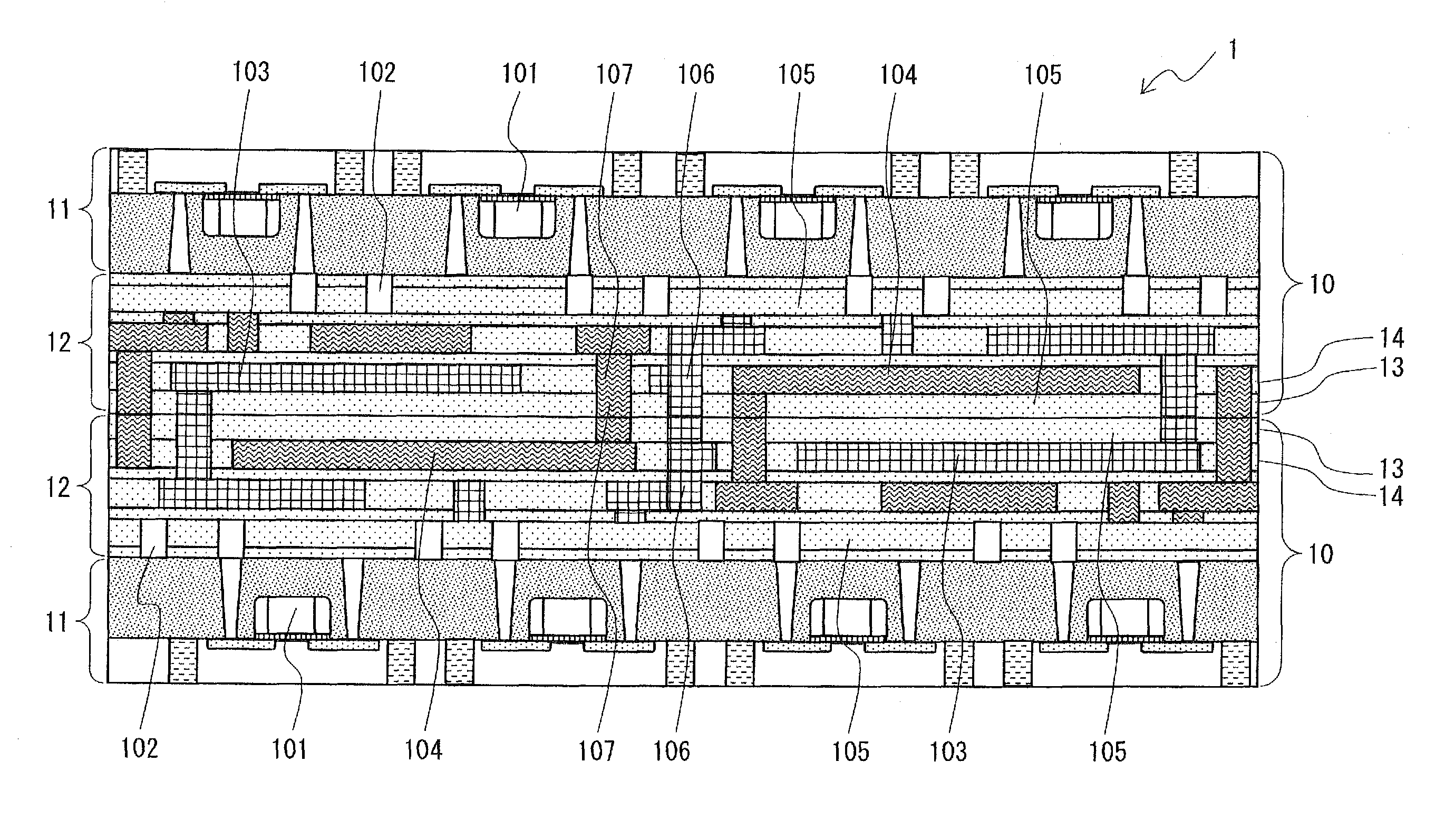
[0027]The following describes a three-dimensional integrated circuit 1 according to an embodiment of the present invention.
[0028]The following describes a process through which the present inventors have arrived at a three-dimensional integrated circuit 1.
[0029]As described above, a decoupling capacitor needs to be arranged in the vicinity of a load so as to achieve its function more effectively. Patent Literature 2 discloses a technique for forming a decoupling capacitor in the vicinity of a load. A semiconductor device according to Patent Literature 2 is reduced in size, and has a structure where a first semiconductor chip including a first conductor layer faces, via an adhesive, a second semiconductor chip including a second conductor layer. In other words, the semiconductor device includes a decoupling capacitor made up of the first conductor layer, the second conductor layer, and the adhesive, where the first and second conductor layers serve as electrodes and the ...
PUM
 Abstract
Description
Claims
Application Information
PatSnap Eureka turns technology decisions into work you can execute. Powered by our Innovation Knowledge Graph, it runs expert workflows across engineering, life sciences, materials and intellectual property. Get your review-ready output in minutes.


