Row Based Analog Standard Cell Layout Design and Methodology

a technology of analog standard cells and layouts, applied in the field of electronic computer-aided design, can solve the problems of inability to teach relatively simple functions of analog standard cells, and the difficulty of pcells such as non-integer-multiple dimensions (variable width and/or height) to be efficiently placed within a soc physical design

Active Publication Date: 2013-02-14
TOTIC TECH INC
View PDF12 Cites 34 Cited by
  • Summary
  • Abstract
  • Description
  • Claims
  • Application Information

AI Technical Summary

Problems solved by technology

While the term analog standard cells exists in prior art, prior art does not define analog standard cells in a manner that accords them significant utility in designing the physical layout of analog or mixed-signal SoCs.
Specifically, prior art has not taught analog standard cells comprising relatively simple functions, predetermined cell heights, inc...

Method used


Image

  • Row Based Analog Standard Cell Layout Design and Methodology
  • Row Based Analog Standard Cell Layout Design and Methodology
  • Row Based Analog Standard Cell Layout Design and Methodology

Examples


Embodiment Construction

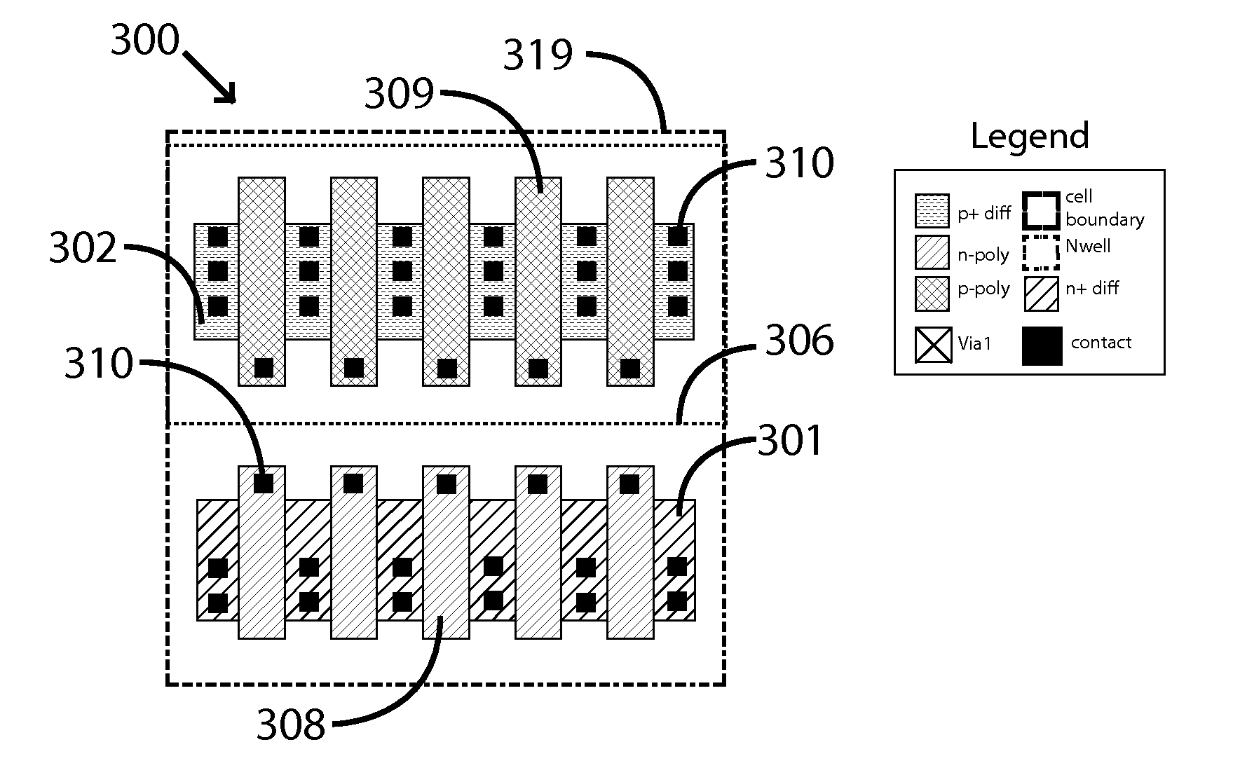
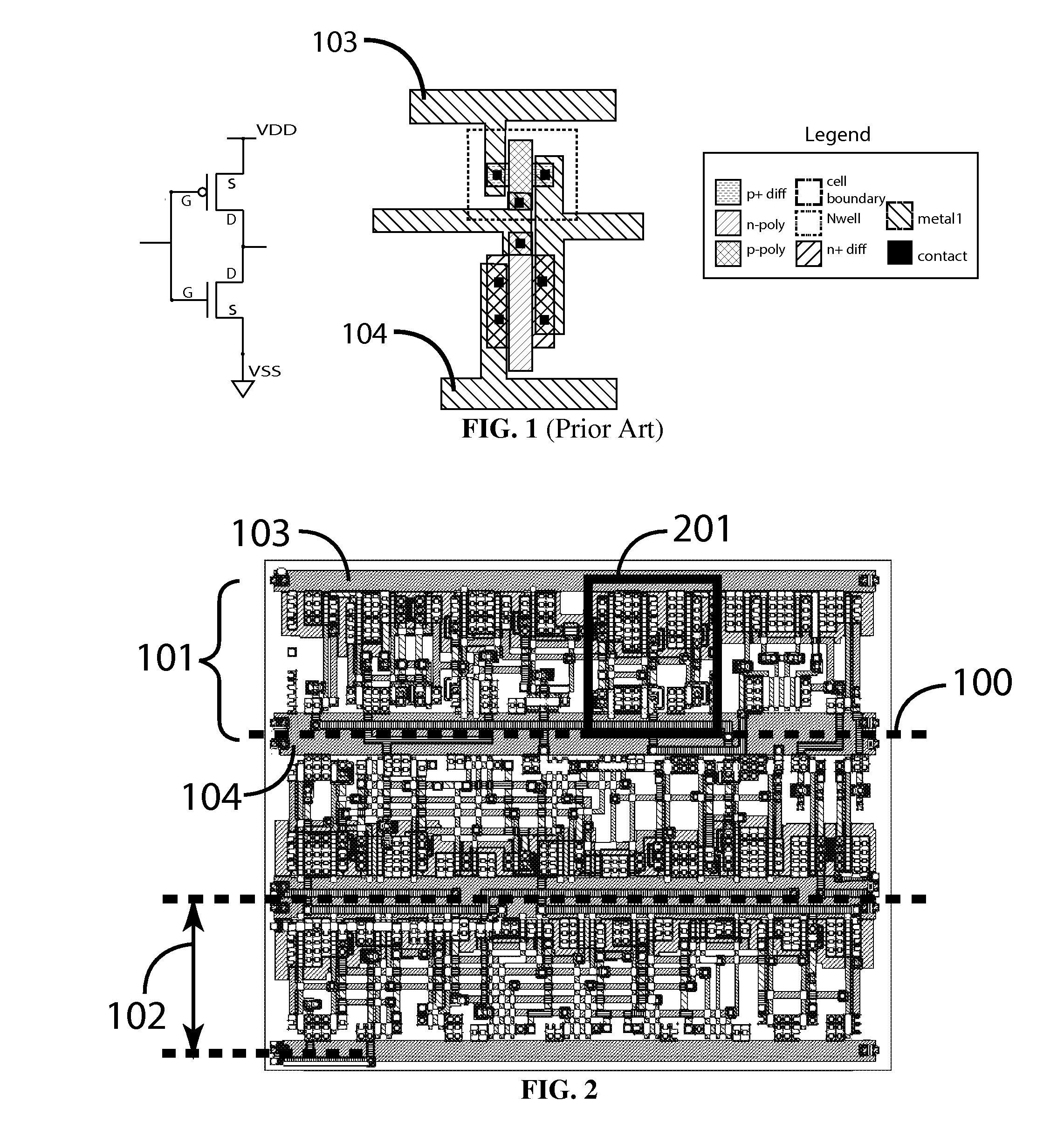
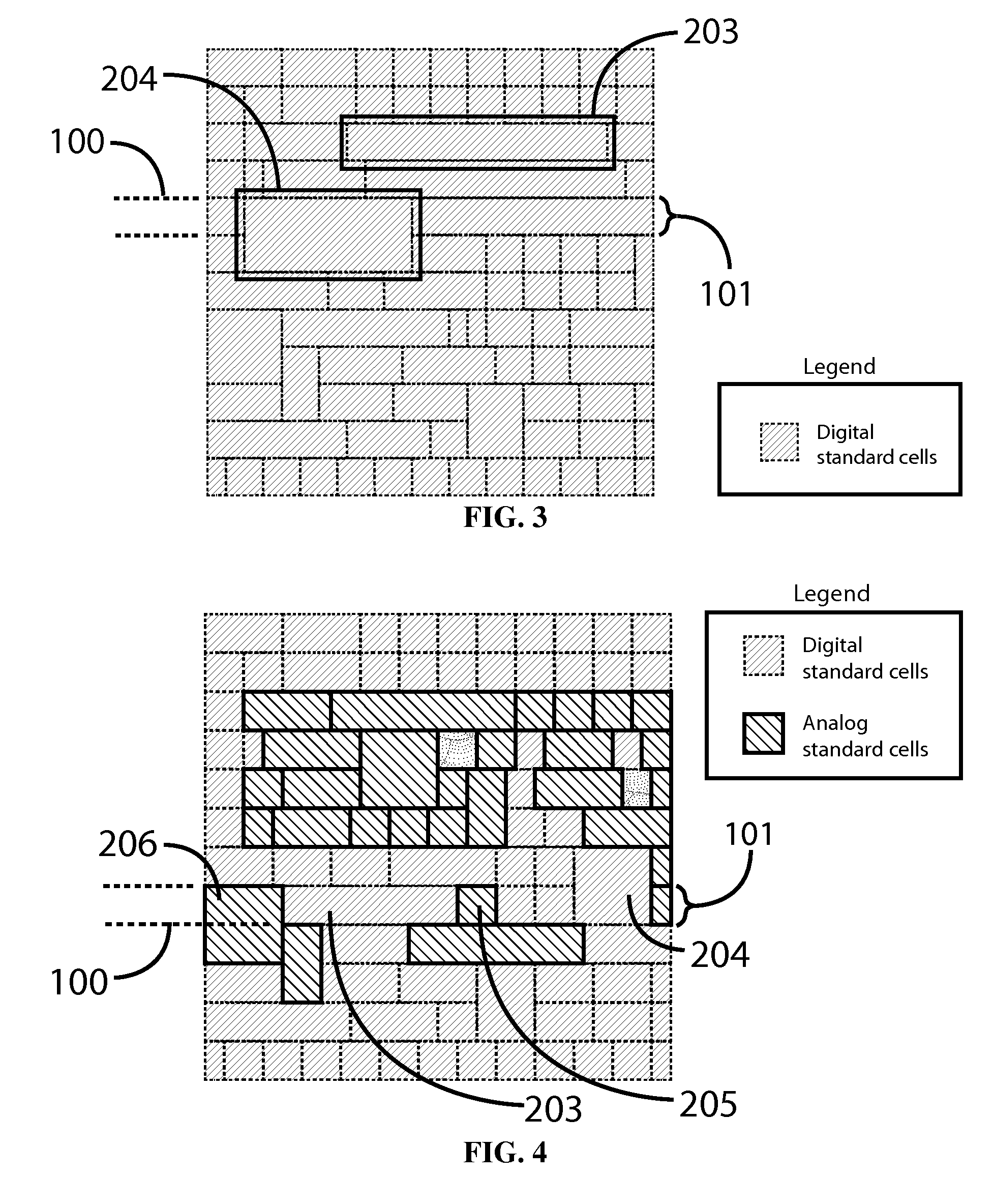
[0024]One major aspect of the well established methodology of designing SoCs is to utilize a library of digital standard cells to layout the physical design. A digital standard cell is generally comprised of a few transistors that perform some logic function. The logic function is typically elementary or simple, for example a logical AND function, a logical OR function, and so on. The left side of FIG. 1 shows an typical CMOS inverter (logical NOT function) and the right side of FIG. 1 shows a corresponding digital standard cell with connections made to the VDD and VSS power rails. By interconnecting the inputs and outputs of multiple digital standard cells, more complex logic functions can be created, thereby forming building blocks of an SoC physical design.

[0025]ECAD tools are used to select standard cells from a library, map the circuitry of an SoC design to standard cells, place standard cells, and route (interconnect) standard cells to create the physical design (the layout). ...


PUM


Abstract

A system and method of designing the physical layout of an SoC incorporating row-based placement of analog standard cells whose heights are constrained to a predetermined row height or integer multiple thereof. A library of analog standard cells may be utilized by an ECAD tool to map, place, and route analog and mixed signal circuits in a manner similar to how such ECAD tool may utilize a library of digital standard cells to map, place, and route digital circuits. Mapping, placing, and routing of digital, analog, and mixed signal circuits may proceed within a unified ECAD SoC physical design flow. Finally, a general type analog standard cell is taught to further increase the speed and efficiency of analog and mixed-signal SoC layout.

Description

CROSS-REFERENCE TO RELATED APPLICATIONS[0001]This application claims the benefit of U.S. Provisional Patent Application No. 61 / 522,692, filed Aug. 12, 2011, by applicant William Loh.BACKGROUND OF THE INVENTION[0002]The present invention relates generally to Electronic Computer-Aided Design (ECAD). More specifically, it pertains to a system and methodology of using analog standard cells, and an analog standard cell library, in a System-on-Chip (SoC) physical design environment. What is taught is a definition of both general and specialized analog standard cells that permit the physical layout of analog and mixed-signal SoCs to be designed quickly and efficiently using ECAD tools.[0003]While the term analog standard cells exists in prior art, prior art does not define analog standard cells in a manner that accords them significant utility in designing the physical layout of analog or mixed-signal SoCs. Specifically, prior art has not taught analog standard cells comprising relatively ...

Claims


Application Information

Patent Timeline
IPC IPC(8): G06F17/50
CPCG06F17/5068G06F17/5063G06F30/36G06F30/39G06F30/373G06F30/392
Inventor LOH, WILLIAMCHMELAR, ERIK VACLAV
Owner TOTIC TECH INC
Why Eureka
Try Eureka