Solder Bump Bonding In Semiconductor Package Using Solder Balls Having High-Temperature Cores

a technology of solder balls and semiconductors, which is applied in the direction of semiconductor devices, semiconductor/solid-state device details, electrical apparatus, etc., can solve the problem that the solder may no longer completely encase or uniformly surround the high-temperature core, and achieve the effect of higher melting temperatur

Inactive Publication Date: 2013-02-21
ADVANCED ANALOGIC TECHNOLOGIES INCORPORATED +1
View PDF12 Cites 19 Cited by
  • Summary
  • Abstract
  • Description
  • Claims
  • Application Information

AI Technical Summary

Benefits of technology

[0021]The die coplanarity problem is avoided in a semiconductor package according to this invention. In a bump-on-leadframe package, an electrical connection between a contact pad on a semiconductor die and a lead comprises solder surface layer and a high-temperature core, the high-temperature core being laterally surrounded by the s

Problems solved by technology

It is also understood that while the solder may substantially surround and encase the high temperature core initially, that during attachment of the die to a leadframe or circuit boa

Method used


Image

  • Solder Bump Bonding In Semiconductor Package Using Solder Balls Having High-Temperature Cores
  • Solder Bump Bonding In Semiconductor Package Using Solder Balls Having High-Temperature Cores
  • Solder Bump Bonding In Semiconductor Package Using Solder Balls Having High-Temperature Cores

Examples


Embodiment Construction

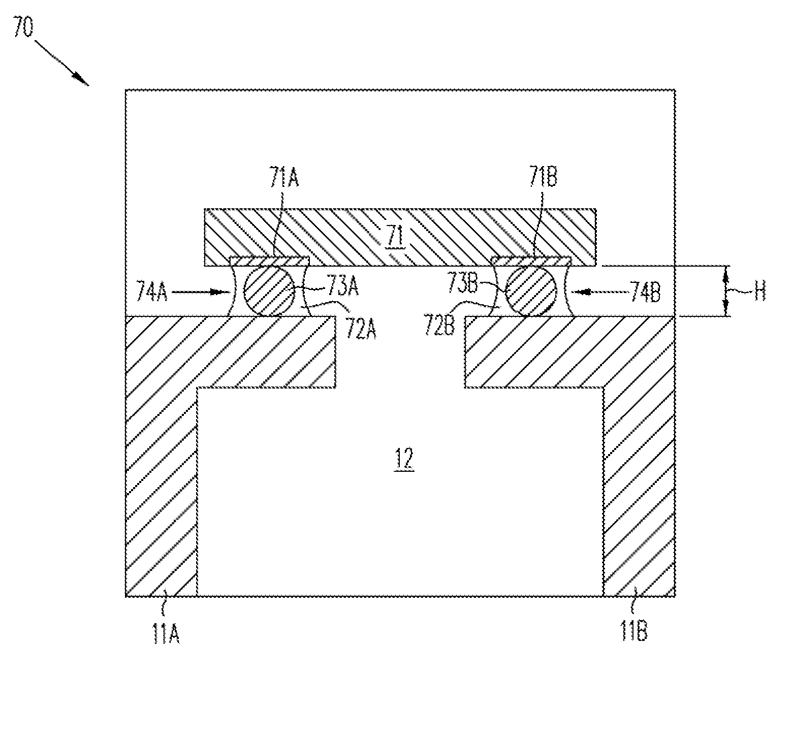
[0036]An exemplary no-lead package 70 in accordance with the invention is shown in FIG. 4. A semiconductor die 71 includes contact pads 71A and 71B. Contact pad 71A is connected to lead 11A by means of an electrical connection 74A. Contact pad 71B is connected to lead 11B by means of an electrical connection 74B. Each of electrical connections 74A and 74B comprises a solder surface layer and a high-temperature core, the high-temperature core being laterally surrounded or substantially surrounded by solder surface layer. Thus, in electrical connection 74A, a high-temperature core 73A is laterally surrounded by a solder surface layer 72A. In electrical connection 74B, a high-temperature core 73B is laterally surrounded by a solder surface layer 72B. Cores 73A and 73B have the same vertical dimension H and are preferably of the same size and shape.

[0037]In many embodiments the high-temperature core will be spherical, as shown by cores 73A and 73B in FIG. 4, but this need not be the cas...


PUM


Abstract

A semiconductor die is solder bump-bonded to a leadframe or circuit board using solder balls having cores made of a material with a melting temperature higher than the melting temperature of the solder to ensure that in the finished structure the die is parallel to the leadframe or circuit board.

Description

CROSS-REFERENCE TO RELATED APPLICATIONS[0001]This application is related to application Ser. No. 11 / 381,292, filed May 2, 2006, titled “Bump-on-Leadframe (BOL) Package Technology with Reduced Parasitics,” which is incorporated herein by reference in its entirety.BACKGROUND OF THE INVENTION[0002]Semiconductor chips or dice typically have contact pads on their surface which provide electrical access to the circuitry within the semiconductor die itself. Since these contact pads are very small, they are normally connected to an external printed circuit board, or the semiconductor die is enclosed within a package having leads that can readily be connected to external circuitry. One technique of making the connection between the contact pads on the die and the printed circuit board or package leads is referred to as “flip-chip” or “solder bump” bonding. With this technique, the die is oriented such that the surface of the die on which the pads are located, normally the top surface, is fac...

Claims


Application Information

Patent Timeline
IPC IPC(8): H01L23/495H01L21/60
CPCH01L23/4334H01L23/49551H01L23/49572H01L2224/16225H01L2224/16245H01L2224/14131H01L2224/13561H01L2224/11005H01L2224/1111H01L2224/13186H01L23/3107H01L24/05H01L24/11H01L24/13H01L24/16H01L24/81H01L2224/11334H01L2224/11505H01L2224/13023H01L2224/13124H01L2224/13147H01L2224/13187H01L2224/1357H01L2224/13582H01L2224/136H01L2224/13611H01L2224/13639H01L2224/13644H01L2224/81191H01L2224/81211H01L2224/94H01L2224/13616H01L2224/05572H01L2224/1112H01L2924/01327H01L2924/10253H01L2224/0401H01L2924/00014H01L2924/00H01L2924/05442H01L2924/014H01L2924/0105H01L2924/00012H01L2224/11H01L2224/05552H01L2924/181
Inventor WILLIAMS, RICHARD K.LIN, KENG HUNG
Owner ADVANCED ANALOGIC TECHNOLOGIES INCORPORATED
Why Eureka
Try Eureka