Light-Emitting Device, Electronic Device, Lighting Device, and Method for Manufacturing the Light-Emitting Device

Active Publication Date: 2013-02-28
SEMICON ENERGY LAB CO LTD
View PDF6 Cites 67 Cited by
  • Summary
  • Abstract
  • Description
  • Claims
  • Application Information

AI Technical Summary

Benefits of technology

[0035]In general, the sealing property of a glass layer is insufficient before the glass layer is irradiated with laser light. Thus, deterioration of an organic EL element due to impurities occurs when a light-emitting device is exposed to the air. In contrast, the fourth step is performed in one embodiment of the present invention, so that the organic EL element is sufficiently sealed with the photocurable resin containing the dry agent and the pair of substrates. Accordingly, entry of impurities such as moisture or oxygen into the light-emitting element to deteriorate the light-emitting element can be suppressed even when the fifth step is performed in the air.
[0036]Further, in the method for manufacturing a light-emitting device, the fourth step is performed under reduced pressure. With the fourth step performed under reduced pressure, the space where the organic EL element is sealed with the photocurable resin containing the dry agent and the pair of substrates keeps its reduced pressure. Thus, the state where pressure

Problems solved by technology

However, in a light-emitting device whose organic EL element is sealed with a pair of glass substrates and glass frit, a sufficient effect of sealing cannot be obtained in some cases because the strength of a glass layer formed with the glass frit is not sufficient or the adhesion strength of the glass frit to a material in contact with the glass fr

Method used


Image

  • Light-Emitting Device, Electronic Device, Lighting Device, and Method for Manufacturing the Light-Emitting Device
  • Light-Emitting Device, Electronic Device, Lighting Device, and Method for Manufacturing the Light-Emitting Device
  • Light-Emitting Device, Electronic Device, Lighting Device, and Method for Manufacturing the Light-Emitting Device

Examples


embodiment 1

[0055](Embodiment 1)

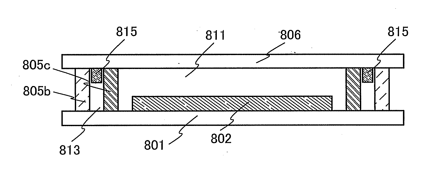
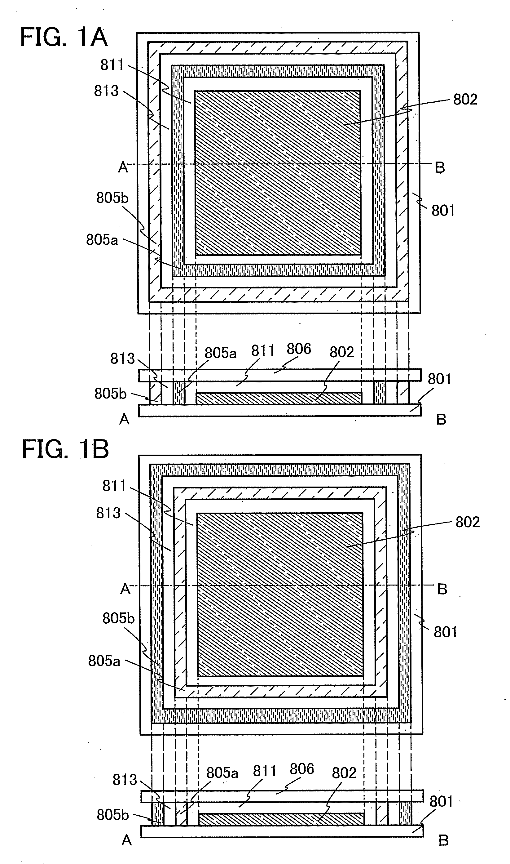
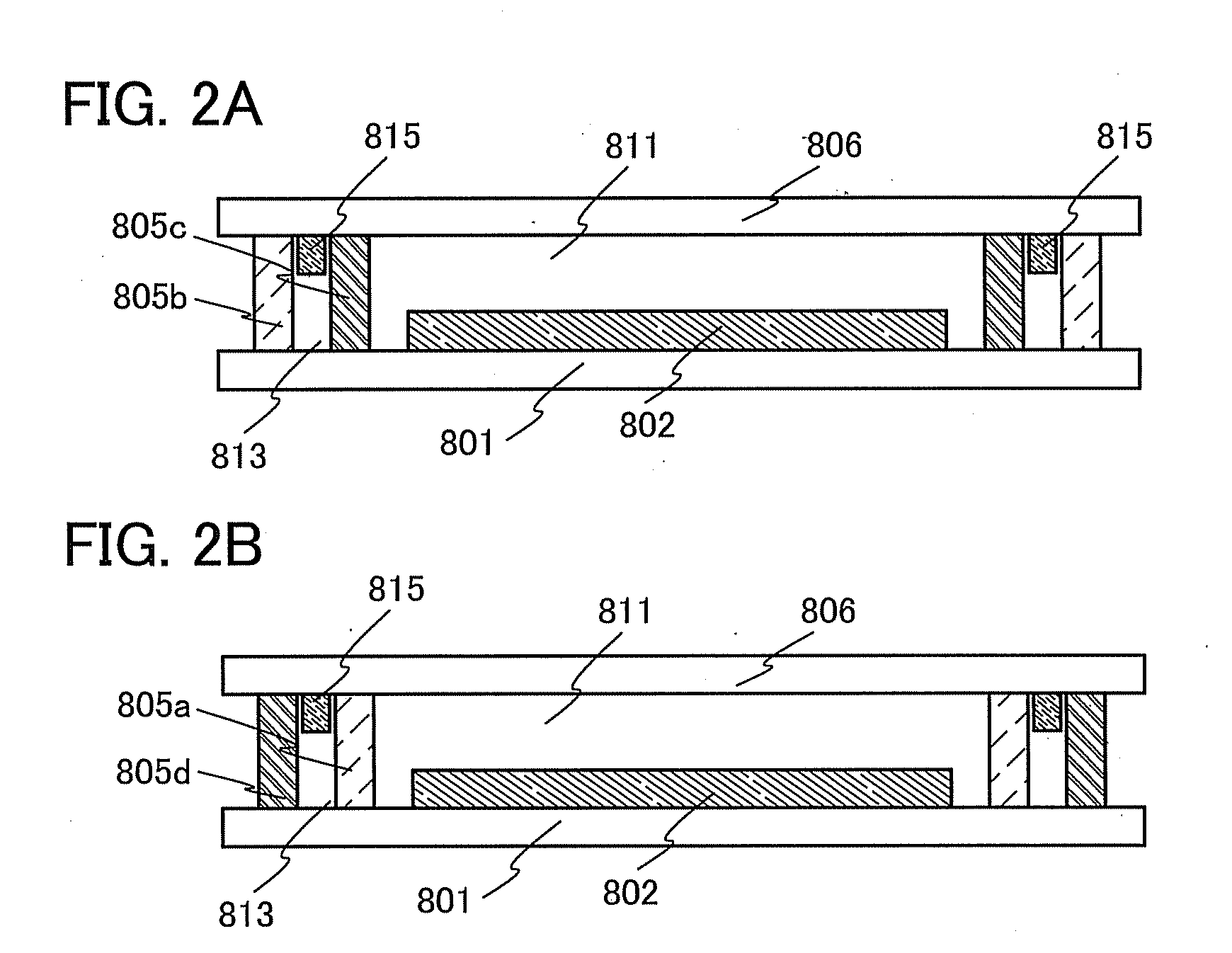
[0056]In this embodiment, light-emitting devices of one embodiment of the present invention will be described with reference to FIGS. 1A and 1B and FIGS. 2A and 2B.

[0057]The light-emitting device of one embodiment of the present invention includes one or more light-emitting elements between a first substrate and a second substrate which face each other. The light-emitting element includes a layer containing a light-emitting organic compound (hereinafter referred to as an EL layer) between a pair of electrodes. The light-emitting element is sealed with a first sealant which is provided along the peripheries of the first substrate and the second substrate to surround the light-emitting element. Further, the light-emitting element is sealed with a second sealant which is provided along the peripheries of the first substrate and the second substrate to surround the first sealant. One of the first sealant and the second sealant is a glass layer and the other is a resi...

embodiment 2

[0119](Embodiment 2)

[0120]In this embodiment, a method for manufacturing a light-emitting device, according to one embodiment of the present invention will be described with reference to FIGS. 3A to 3C and FIGS. 4A to 4C. In particular, Structural Example 2 (see FIG. 1B) described in Embodiment 1 will be described as an example.

[0121]{First Step: Formation of Light-Emitting Portion}

[0122]The light-emitting portion 802 is formed over the first substrate 801 (FIG. 3A). Specifically, the organic EL element, a transistor for controlling light emission of the organic EL element, and the like included in the light-emitting portion 802 are formed. In the case of an active matrix light-emitting device, a driver circuit portion or the like may be provided in addition to the light-emitting portion 802. A structural example of the active matrix light-emitting device will be described in detail in Embodiment 3.

[0123]{Second Step: Formation of Sealant 1 Glass Layer}

[0124]In this embodiment, the ...

embodiment 3

[0162](Embodiment 3)

[0163]In this embodiment, a light-emitting device of one embodiment of the present invention will be described with reference to FIGS. 5A and 5B. FIG. 5A is a plan view of the light-emitting device of one embodiment of the present invention and FIG. 5B is a cross-sectional view taken along dashed-dotted line E-F in FIG. 5A.

[0164]An active matrix light-emitting device according to this embodiment includes, over the first substrate 801, the light-emitting portion 802, a driver circuit portion 803 (gate side driver circuit portion), and a driver circuit portion 804 (source side drive circuit portion). The first sealant 805a is provided so as to surround the light-emitting portion 802, the driver circuit portion 803, and the driver circuit portion 804, and the second sealant 805b is provided so as to surround the first sealant 805a. Thus, the light-emitting portion 802 and the driver circuit portions 803 and 804 are sealed in the second space 811 surrounded by the fi...


PUM


Abstract

A light-emitting device in which deterioration of an organic EL element due to impurities such as moisture or oxygen is suppressed is provided. The light-emitting device includes a first substrate and a second substrate facing each other, a light-emitting element provided over the first substrate, a first sealant provided so as to surround the light-emitting element, and a second sealant provided so as to surround the first sealant. One of the first sealant and the second sealant is a glass layer and the other is a resin layer. A dry agent is provided in a first space surrounded by the first sealant, the second sealant, the first substrate, and the second substrate, or in the resin layer. The light-emitting element is included in a second space surrounded by the first sealant, the first substrate, and the second substrate.

Description

TECHNICAL FIELD[0001]The present invention relates to a light-emitting device, an electronic device, and a lighting device each using organic electroluminescence (EL). The present invention also relates to a method for manufacturing the light-emitting device.BACKGROUND ART[0002]A light-emitting element (also referred to as an organic EL element) using organic EL has been actively researched and developed. In the fundamental structure of an organic EL element, a layer containing a light-emitting organic compound is provided between a pair of electrodes. By voltage application to this element, light emission from the light-emitting organic compound can be obtained.[0003]An organic EL element, which has characteristics such as feasibility of being thinner and lighter, high speed response to input signals, and capability of direct current low voltage driving, has been expected to be applied to next-generation flat panel displays or lighting devices. In particular, a display device in wh...

Claims


Application Information

Patent Timeline
IPC IPC(8): H01L51/50H01L51/46H01L33/54
CPCH05B33/04H01L51/5068H01L51/5246H01L2251/566H01L27/322H01L27/3244H01L51/5259H10K59/38H10K59/12H10K50/157H10K50/846H10K50/8426H10K71/851H10K71/00
Inventor NISHIDO, YUSUKEYAMAZAKI, SHUNPEI
Owner SEMICON ENERGY LAB CO LTD
Why Eureka
Try Eureka