

Power supply device
- Summary
- Abstract
- Description
- Claims
- Application Information
AI Technical Summary
Benefits of technology
Problems solved by technology
Method used
Image

Examples
embodiment 1
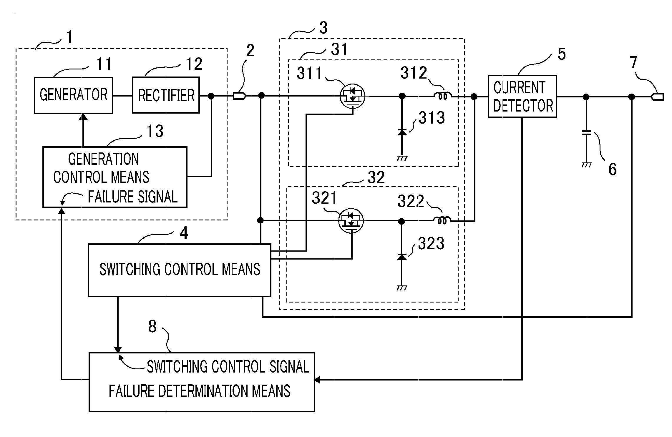
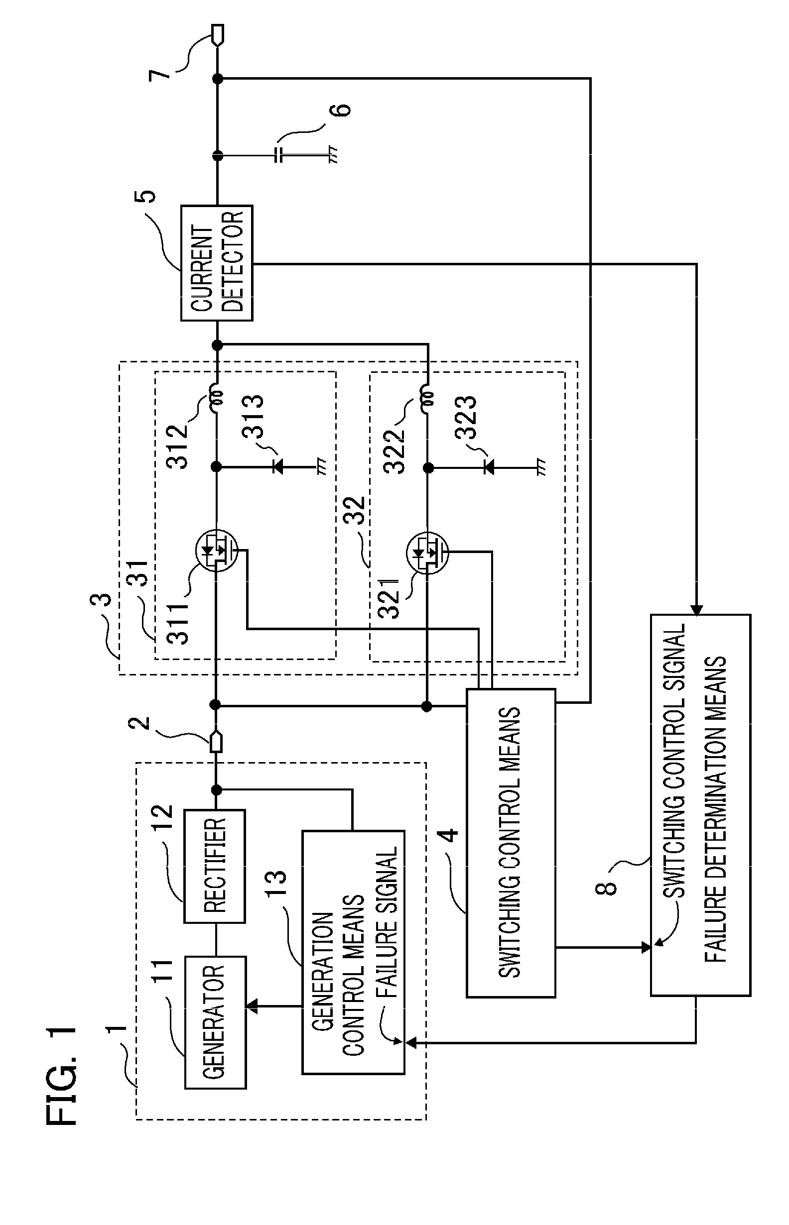
[0026]FIG. 1 is a block diagram showing the configuration of a power supply device according to Embodiment 1 of the present invention.
[0027]In the figure, the power supply device comprises: a power generation unit 1 including a generator 11 and a generation control means 13 for controlling the generator 11 when a DC voltage obtained by rectifying by a rectifier 12 an AC voltage output from the generator 11 exceeds an acceptable range of a setting voltage; a multiphase chopper 3 including a first-phase chopper section 31 that is made up of a switching element 311 that is connected to an input terminal 2 connected to the power generation unit 1 and driven in switched mode, a rectifying element 313 whose anode and cathode are connected to ground and the output end of the switching element 311, respectively, and a reactor 312 that is connected to the output end of the switching element 311 and smoothes an input voltage converted by the switching element 311 and the rectifying element 31...
embodiment 2
[0060]FIG. 8 is a block diagram showing an example of a multiphase chopper of a power supply device according to Embodiment 2 of the present invention being constituted of three-phase chopper sections, which in addition to the first chopper section 31 and second chopper section 32 of Embodiment 1, includes a third chopper section 33 configured the same as these chopper sections. In this configuration, the switching control means 4 outputs control signals that are shifted by 120° in phase with each other to the switching elements 311, 321 and 331 (not shown in the figure) of the respective phase chopper sections 31, 32 and 33.
[0061]The control signals to the switching elements of the chopper sections 31, 32 and 33 and their currents before and after a failure will be explained. Assume that an open-circuit failure occurs in the switching element 321 of the second-phase chopper section 32.
[0062]FIG. 9 shows currents with respect to time before the switching element 321 fails. IL repres...
embodiment 3
[0068]FIG. 11 is a block diagram showing the configuration of a power supply device according to Embodiment 3 of the present invention.
[0069]The power supply device is configured in a way such that the failure determination means 8 transmits a failure signal to the switching control means 4, and the switching control means 4, when receiving the failure signal, obtains values of the reactor current IL detected by the current detector 5 and adjusts a duty ratio for switching elements of non-failed chopper sections of the phases so that their withstanding current is not exceeded.
[0070]FIG. 12 is a flowchart showing the operation of the switching control means according to Embodiment 3 of the invention. Before a switching element fails, Steps S81 to S87 shown in FIG. 5 are executed the same as Embodiment 1. Here, when a switching element fails, the failure determination means 8 transmits a failure signal to the switching control means 4 after the completion of Step S85 in FIG. 5. After ...
PUM
 Abstract
Description
Claims
Application Information