Substrate and Patterning Device for Use in Metrology, Metrology Method and Device Manufacturing Method

a patterning device and metrology technology, applied in semiconductor/solid-state device details, printing, instruments, etc., can solve the problems of limited accuracy with which overlays and other parameters are measured, large targets, and insufficient realization of the benefit of measuring overlays or other parameters within product areas

Active Publication Date: 2013-03-07
ASML NETHERLANDS BV
View PDF1 Cites 36 Cited by
  • Summary
  • Abstract
  • Description
  • Claims
  • Application Information

AI Technical Summary

Benefits of technology

[0008]Therefore, what is needed is a system and method for present invention using small target metrology to measure parameters for example at locations within product areas on a semiconductor substrate, with an accuracy similar to that associated with larger targets.

Problems solved by technology

Unfortunately, the nature of the small targets and the techniques required to measure them tends to limit the accuracy with which overlay and other parameters can be made, making it lower than can be achieved with conventional, larger targets.
Therefore the benefit of measuring overlay or other parameters within product areas is not fully realized, because the accuracy of the small target measurements themselves is impaired.

Method used


Image

  • Substrate and Patterning Device for Use in Metrology, Metrology Method and Device Manufacturing Method
  • Substrate and Patterning Device for Use in Metrology, Metrology Method and Device Manufacturing Method
  • Substrate and Patterning Device for Use in Metrology, Metrology Method and Device Manufacturing Method

Examples


Embodiment Construction

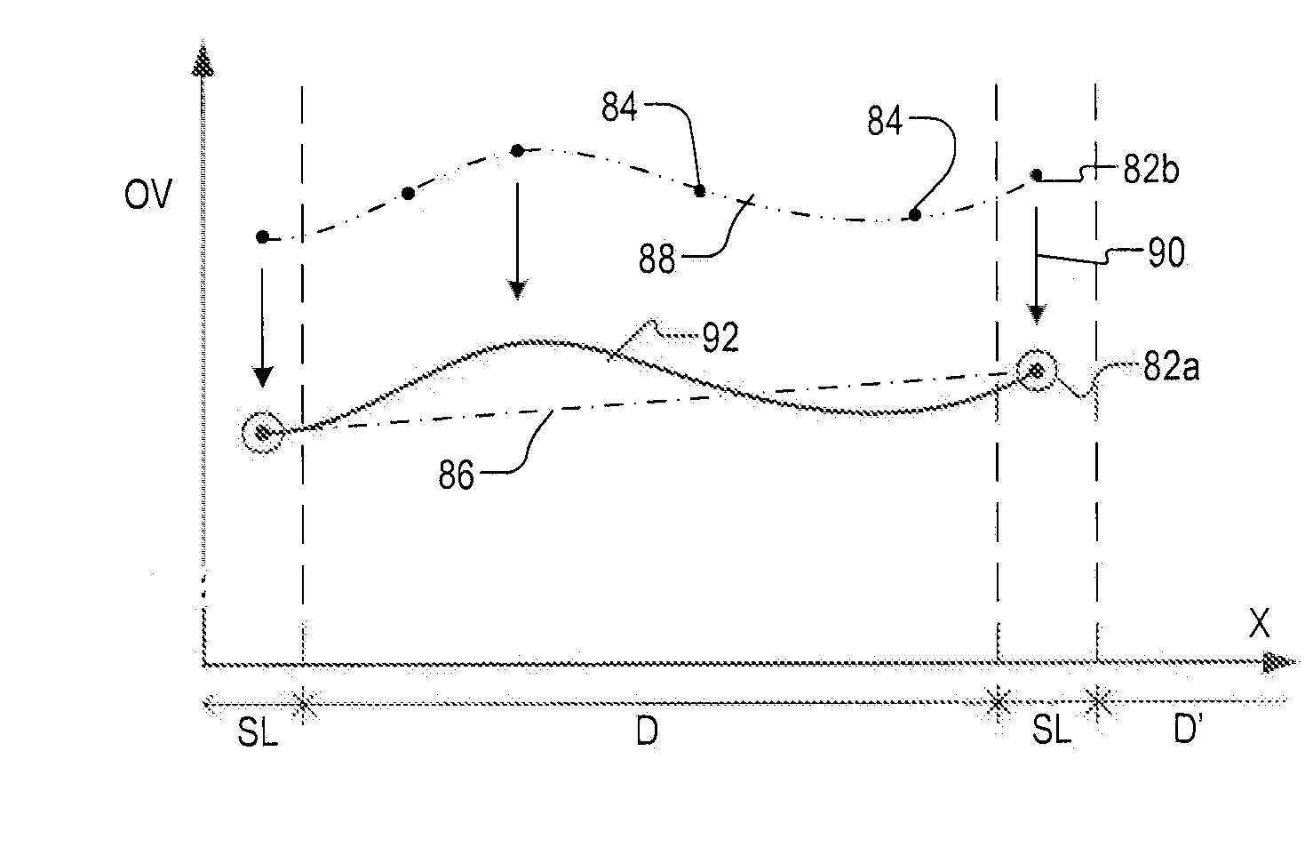
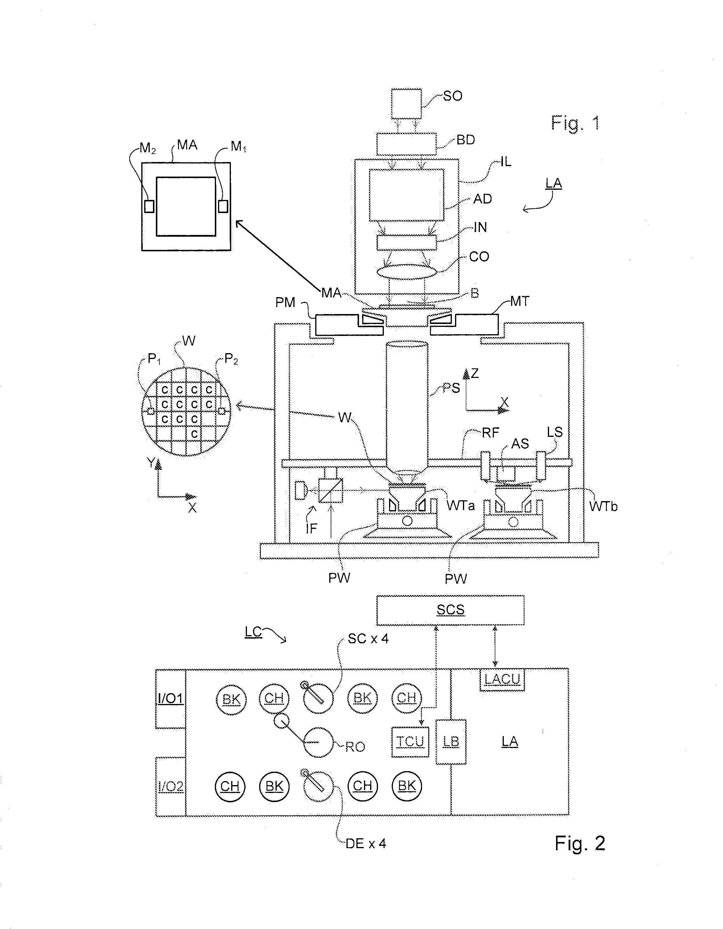
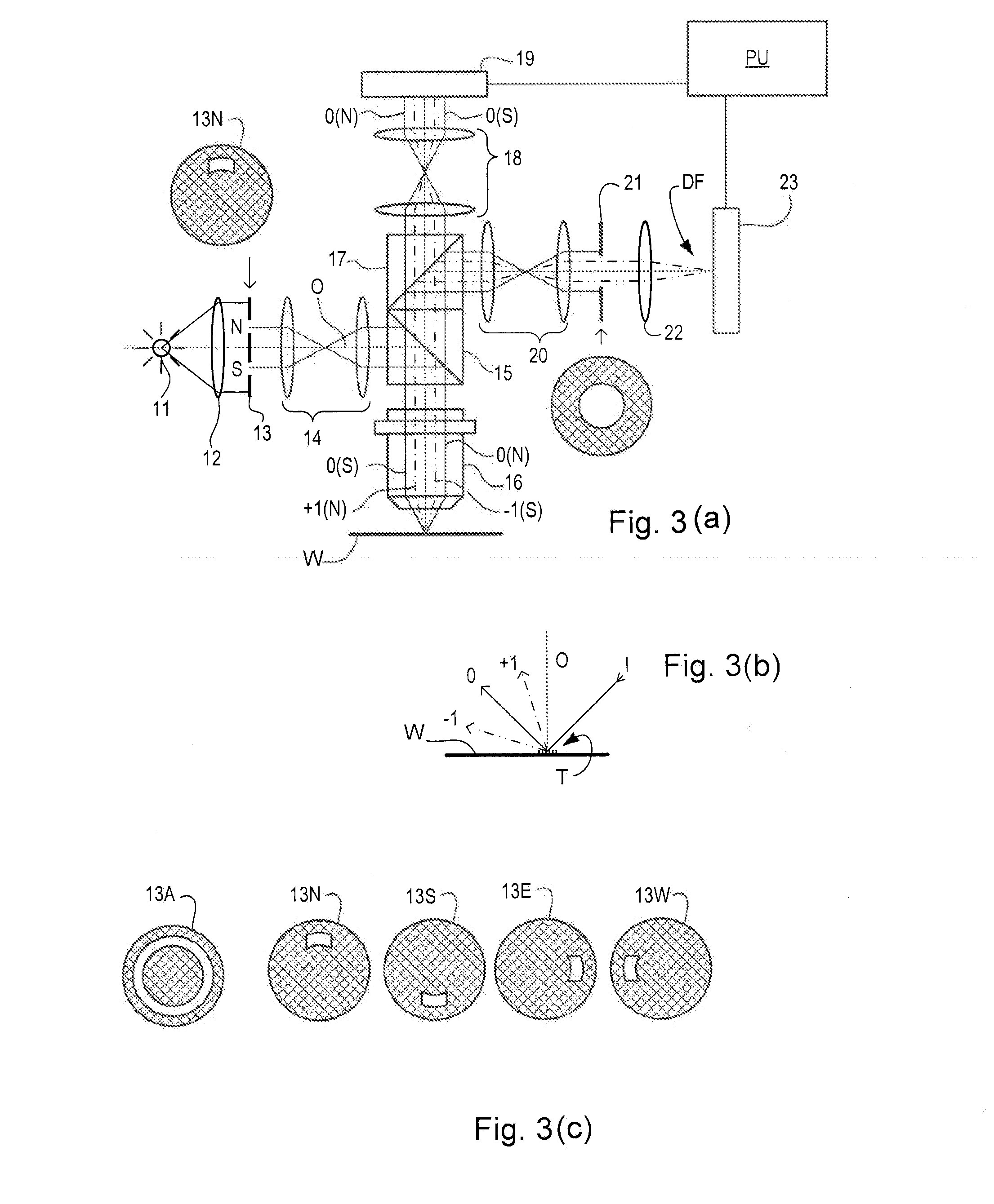
[0029]This specification discloses one or more embodiments that incorporate the features of this invention. The disclosed embodiment(s) merely exemplify the invention. The scope of the invention is not limited to the disclosed embodiment(s). The invention is defined by the claims appended hereto.

[0030]The embodiment(s) described, and references in the specification to “one embodiment”, “an embodiment”, “an example embodiment”, etc., indicate that the embodiment(s) described may include a particular feature, structure, or characteristic, but every embodiment may not necessarily include the particular feature, structure, or characteristic. Moreover, such phrases are not necessarily referring to the same embodiment. Further, when a particular feature, structure, or characteristic is described in connection with an embodiment, it is understood that it is within the knowledge of one skilled in the art to effect such feature, structure, or characteristic in connection with other embodimen...


PUM

PropertyMeasurementUnit
sizeaaaaaaaaaa
wavelengthaaaaaaaaaa

Abstract

A pattern from a patterning device is applied to a substrate by a lithographic apparatus. The applied pattern includes product features and metrology targets. The metrology targets include large targets and small targets which are for measuring overlay. Some of the smaller targets are distributed at locations between the larger targets, while other small targets are placed at the same locations as a large target. By comparing values measured using a small target and large target at the same location, parameter values measured using all the small targets can be corrected for better accuracy. The large targets can be located primarily within scribe lanes while the small targets are distributed within product areas.

Description

CROSS REFERENCE TO RELATED APPLICATIONS[0001]This application claims the benefit under 35 U.S.C. §119(e) to U.S. Provisional Application 61 / 467,080, filed Mar. 24, 2011, which is incorporated by reference herein in its entirety.BACKGROUND[0002]1. Field of the Invention[0003]The present invention relates to methods and apparatus for metrology usable, for example, in the manufacture of devices by lithographic techniques and to methods of manufacturing devices using lithographic techniques. Methods of measuring overlay are described, as a particular application of such metrology.[0004]2. Background Art[0005]A lithographic apparatus is a machine that applies a desired pattern onto a substrate, usually onto a target portion of the substrate. A lithographic apparatus can be used, for example, in the manufacture of integrated circuits (ICs). In that instance, a patterning device, which is alternatively referred to as a mask or a reticle, may be used to generate a circuit pattern to be form...

Claims


Application Information

Patent Timeline
Patent Type & Authority Applications(United States)
IPC IPC(8): G01B11/14G03F7/20G03B27/00
CPCG03F7/70633G03F7/70616G01B11/14G03F7/70683H01L2924/0002H01L2924/00H01L23/544H01L23/58G03F9/7042
Inventor VAN DER SCHAAR, MAURITSWARNAAR, PATRICKBHATTACHARYYA, KAUSTUVESMILDE, HENDRIK JAN HIDDEKUBIS, MICHAEL
Owner ASML NETHERLANDS BV
Why Eureka
Try Eureka