Heat dissipating structure of electronic apparatus

a technology of electronic devices and heat dissipation structures, applied in the direction of cooling/ventilation/heating modifications, semiconductor devices, semiconductor/solid-state device details, etc., can solve the problems of electronic component failure, device malfunction, serious heat problem, etc., and achieve the effect of sufficient heat dissipation and improving the reliability of the electronic devi

Inactive Publication Date: 2013-03-14
SHARP KK
View PDF4 Cites 4 Cited by
  • Summary
  • Abstract
  • Description
  • Claims
  • Application Information

AI Technical Summary

Benefits of technology

[0034]According to the present invention, in the heat dissipation structure of dissipating heat through the heat dissipation sheet disposed between the IC chip, which is a heat-generating element, mounted on the substrate, and the cover member, the softer heat dissipation sheet and the harder heat dissipation sheet are laminated in a direction of a gap between the IC chip and the cover member. Therefore, even if variation in gaps between the respective IC chips and the cover member is generated, it is possible to allow the heat dissipation sheet to come in contact with each IC chip and with the cover member with appropriate pressure. As a result, a heat dissipation structure of an electronic device that can dissipate heat sufficiently and that can improve reliability of the electronic device can be achieved.

Problems solved by technology

Arranging the electronic components such as IC chips densely in a small space results in a serious heat problem that requires a measure to dissipate heat.
This may cause device malfunction and electronic component failure.

Method used


Image

  • Heat dissipating structure of electronic apparatus
  • Heat dissipating structure of electronic apparatus
  • Heat dissipating structure of electronic apparatus

Examples


embodiment 2

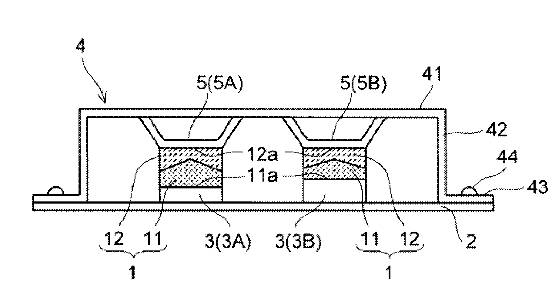
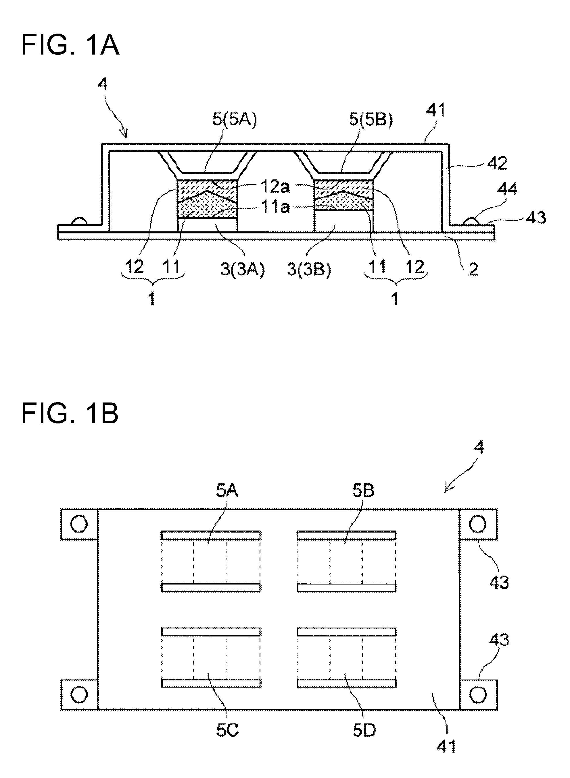
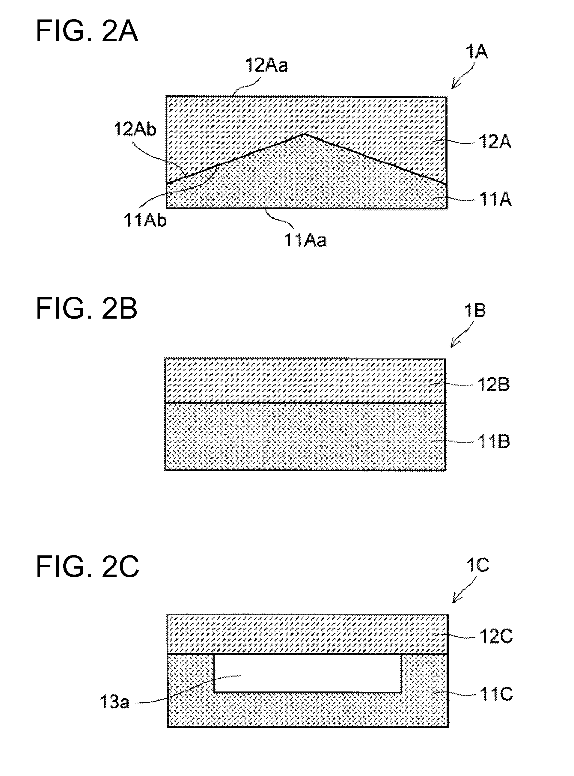
[0071]Further, depending on the area and the thickness of the heat dissipation sheet, the heat dissipation sheet may have a plate-like multilayer structure of Embodiment 2 as shown in FIG. 2B. The multilayer structure may be a structure shown in a heat dissipation sheet 1B in which a harder first heat dissipation sheet 11B and a softer second heat dissipation sheet 12B are simply laminated.

[0072]With the above configuration, the heat dissipation sheet 1B can be easily pressed on the IC chip by the softer second heat dissipation sheet 12B. Further, the overlying harder heat dissipation sheet prevents the softer second heat dissipation sheet 12B from being deformed, and the contact pressure of the heat dissipation sheet 1B on the IC chip is prevented from being excessively decreased. Therefore, the heat dissipation sheet can come in contact with the IC chip with appropriate pressure.

[0073]The heat dissipation sheet 1A of Embodiment 1 and the heat dissipation sheet 1B of Embodiment 2 d...

embodiment 3

[0074]A heat dissipation sheet 1C of Embodiment 3 shown in FIG. 2C has a recess 13a in the center of a bonding surface of a harder first heat dissipation sheet 11C. The recess 13a has a size that substantially coincides with that of the IC chip on which the heat dissipation sheet is to be placed. A softer second heat dissipation sheet 12C has a plate-like shape. This results in a structure in which a hollow in a size that corresponds to that of the IC chip is formed in the center of a bonding portion where the first and second heat dissipation sheets are bonded to each other.

[0075]With the above multilayer structure of having the hollow in a size that substantially coincides with that of the IC chip on which the heat dissipation sheet 1C is to be placed, the softer heat dissipation sheet 12C is pressed on the IC chip with appropriate pressure. Also, because a region outside of the hollow in the softer heat dissipation sheet 12C is bonded to the harder heat dissipation sheet 11C, the...

embodiment 4

[0076]A heat dissipation sheet 1D of Embodiment 4 shown in FIG. 2D is made of a first heat dissipation sheet 11D and a second heat dissipation sheet 12D. Respective bonding surfaces of the first heat dissipation sheet 11D and the second heat dissipation sheet 12D are substantially flat. In the center of a contact surface of the softer second heat dissipation sheet, a recess 13b is made. The recess 13b has a size that substantially coincides with that of a protrusion of the IC chip on which the heat dissipation sheet is to be placed.

[0077]With this configuration, the softer second heat dissipation sheet 12D can be attached to cover the IC chip with the recess 13b that has a size that substantially coincides with that of the protrusion of the IC chip on which the heat dissipation sheet 1D is to be placed. Further, a region outside of the recess 13b in the softer heat dissipation sheet 12D is bonded to the harder first heat dissipation sheet 11D. As a result, the softer second heat dis...


PUM


Abstract

Disclosed is a heat dissipation structure of an electronic device that has an IC chip that is a heat generating element mounted on a substrate and a heat dissipation sheet disposed between the IC chip and a cover member so as to dissipate heat. In such a heat dissipation structure, even if variation in a gap between the IC chip and the cover member is generated, the heat dissipation sheet can come in contact with the IC chip and with the cover member with appropriate pressure. This way, heat is sufficiently dissipated, and therefore, reliability of the electronic device can be improved. A heat dissipation sheet (1) has a double-layered structure in which a first heat dissipation sheet (11) and a second heat dissipation sheet (12) are laminated in a thickness direction. A rubber hardness of the first heat dissipation sheet is set different from that of the second heat dissipating sheet, and a softer heat dissipation sheet and a harder heat dissipation sheet are laminated in a direction of the gap between an IC chip (3) and a cover member (4).

Description

TECHNICAL FIELD[0001]The present invention relates to a heat dissipation structure of an electronic device used for a liquid crystal display device and the like.BACKGROUND ART[0002]In recent years, electronic devices that are provided with substrates having electronic components such as IC chips (semiconductor chips) mounted thereon have been widely available. On substrates for driving liquid crystal display panels of liquid crystal display devices, for example, large numbers of such electronic components are mounted.[0003]The density of the electronic components that are used in various electronic devices has been increased in order to respond to sizes of the electronic devices being reduced. Arranging the electronic components such as IC chips densely in a small space results in a serious heat problem that requires a measure to dissipate heat.[0004]The electronic components such as IC chips mounted on the substrate undergo change in characteristics due to increase in temperature c...

Claims


Application Information

Patent Timeline
Patent Type & Authority Applications(United States)
IPC IPC(8): H05K7/20
CPCH01L23/433H05K7/20454H01L2924/0002H01L2924/00
Inventor KURODA, TATSURO
Owner SHARP KK
Why Eureka
Try Eureka