

Photoelectric conversion device
a conversion device and photoelectric technology, applied in the direction of solid-state devices, semiconductor devices, electrical devices, etc., can solve the problem of difficult to extract a large current from the light absorbing layer, and achieve the effect of enhancing photoelectric conversion efficiency
- Summary
- Abstract
- Description
- Claims
- Application Information
AI Technical Summary
Benefits of technology
Problems solved by technology
Method used
Image

Examples
Embodiment Construction
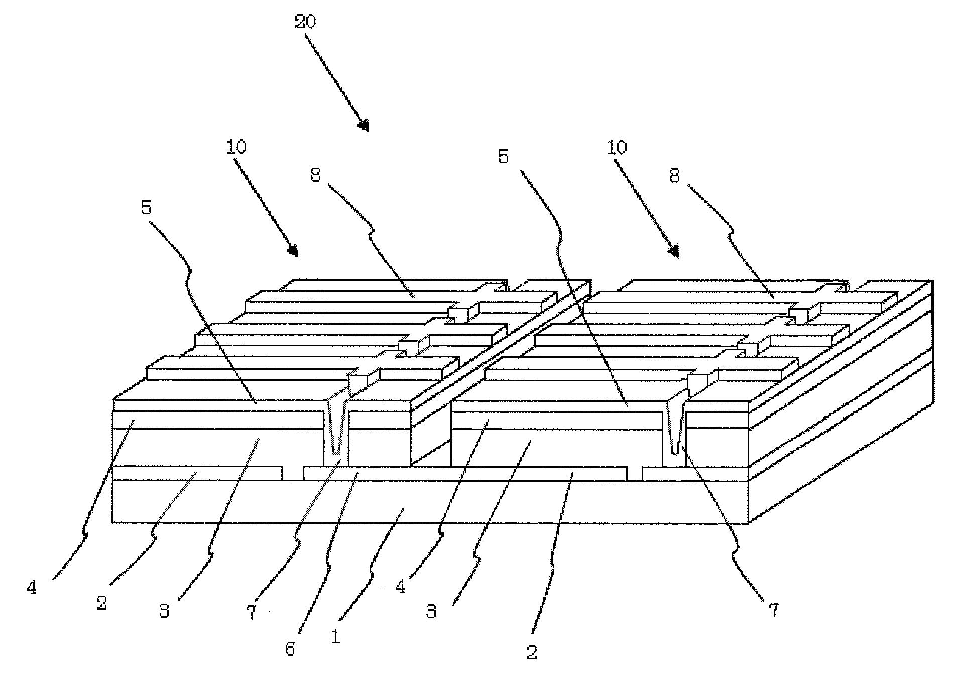
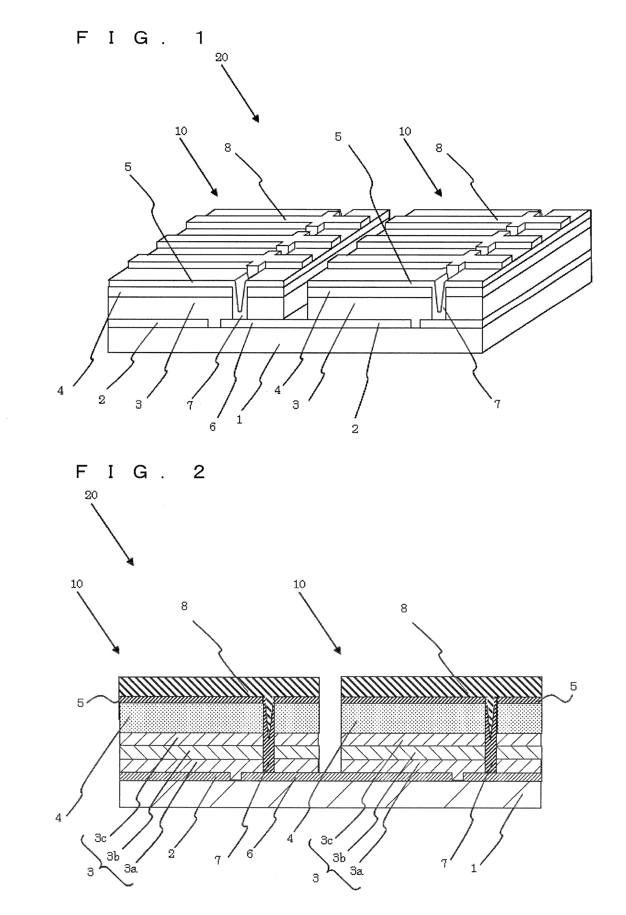
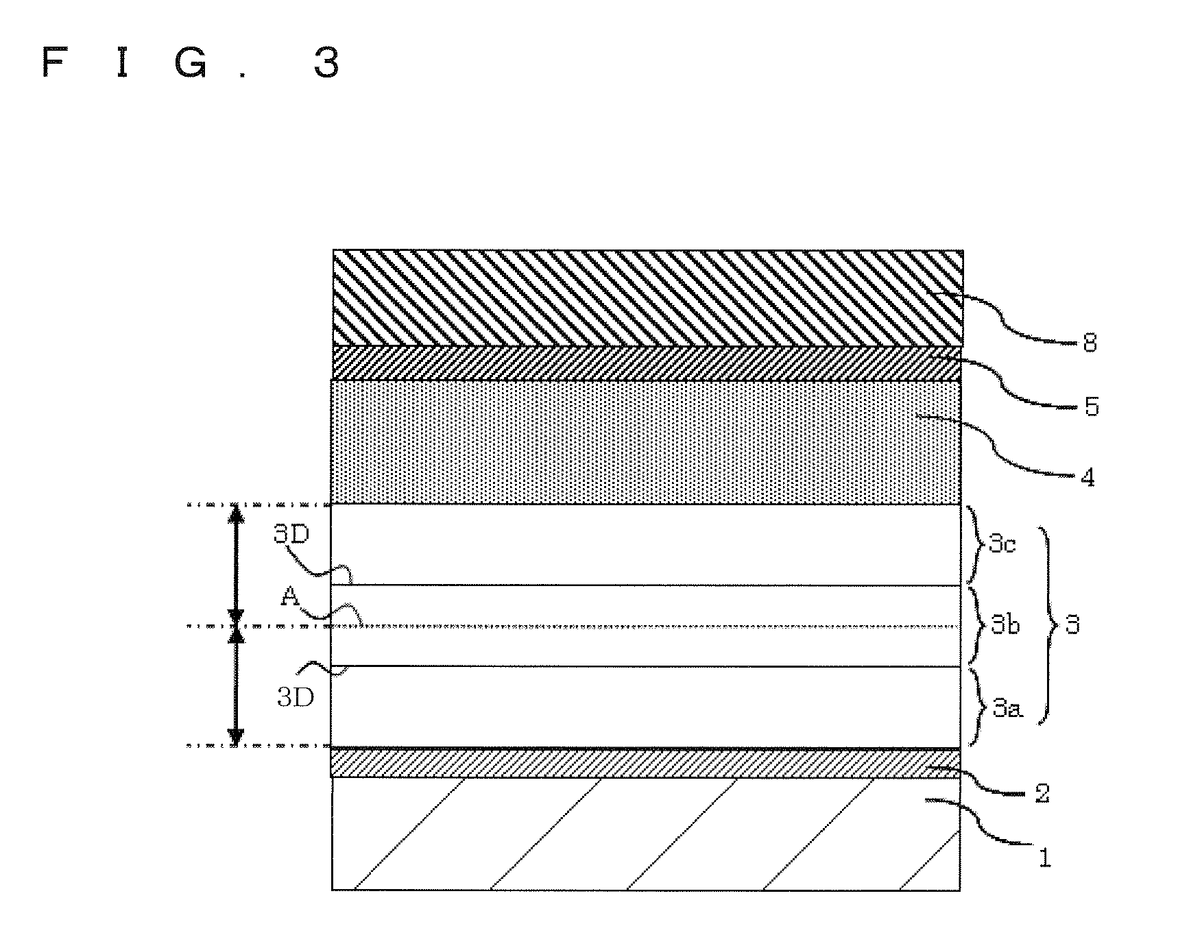
[0010]As shown in FIG. 1, photoelectric conversion devices 10 each include a substrate 1, a first electrode layer 2, a light absorbing layer 3, a buffer layer 4, and a second electrode layer 5. The photoelectric conversion devices 10 include a third electrode layer 6 spaced apart from the first electrode layer 2 and located on a side of the light absorbing layer 3 close to the substrates 1. The photoelectric conversion devices 10 adjacent to each other are electrically connected through a connecting conductor 7. To be specific, the second electrode layer 5 of one of the photoelectric conversion devices 10 is connected through the connecting conductor 7 to the third electrode layer 6 of the other photoelectric conversion device 10. The third electrode layer 6 also functions as the first electrode layer 2 of the adjacent photoelectric conversion device 10, thereby forming series connection between the adjacent photoelectric conversion devices 10. In one photoelectric conversion device...
PUM
 Abstract
Description
Claims
Application Information