Controllable optical device and the forming method thereof

Inactive Publication Date: 2013-04-11
NATIONAL CHIAO TUNG UNIVERSITY
View PDF6 Cites 6 Cited by
  • Summary
  • Abstract
  • Description
  • Claims
  • Application Information

AI Technical Summary

Benefits of technology

[0011]Another purpose of the invention is to provide a controllable optical device, it is lig

Problems solved by technology

The shortcoming of the method is that it is heavier and larger than current optical focus-changing lens set.
However, thicker liquid crystal layer will cause longer response time.
However, it needs extra circuit for

Method used


Image

  • Controllable optical device and the forming method thereof
  • Controllable optical device and the forming method thereof
  • Controllable optical device and the forming method thereof

Examples


Embodiment Construction

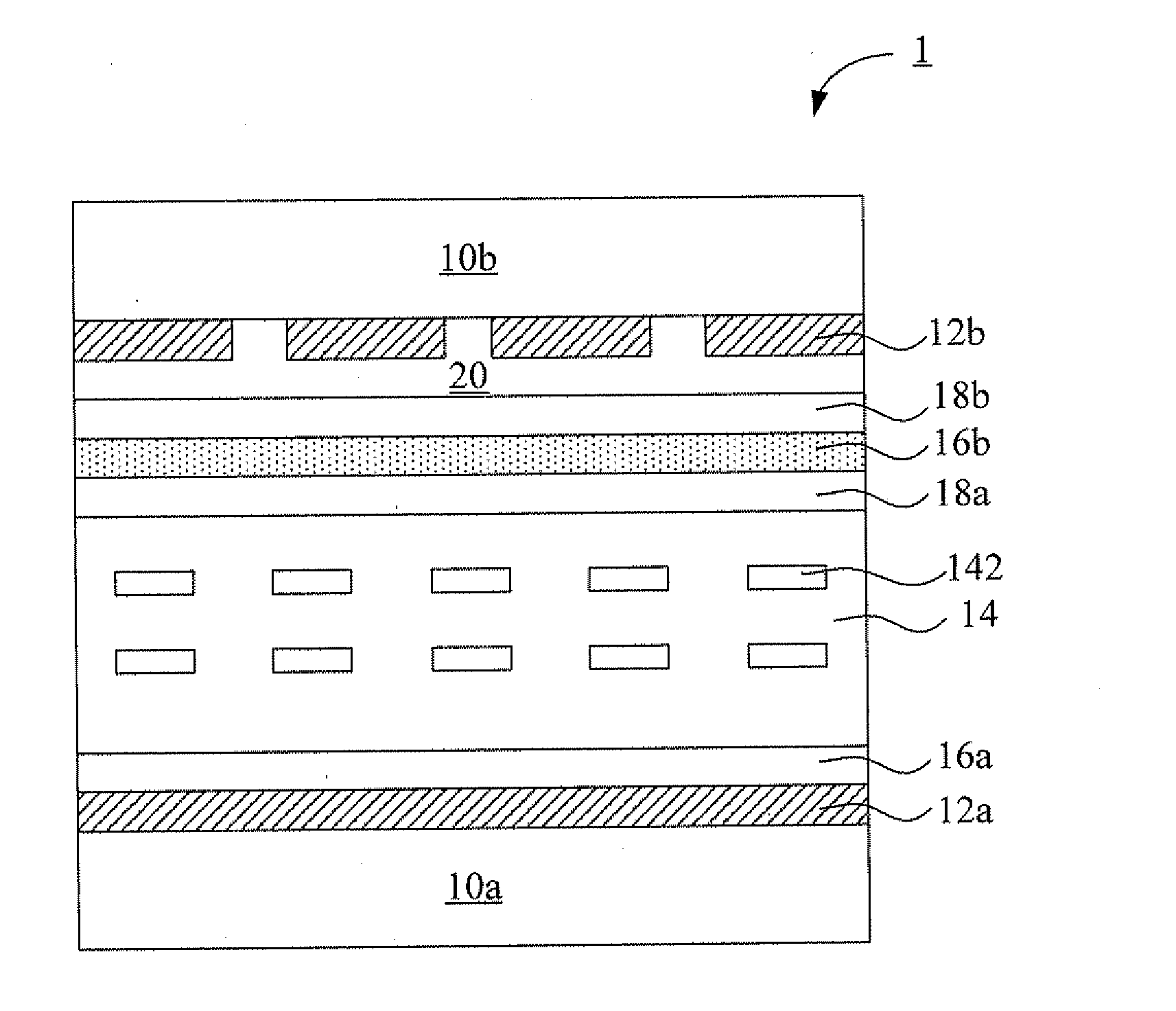
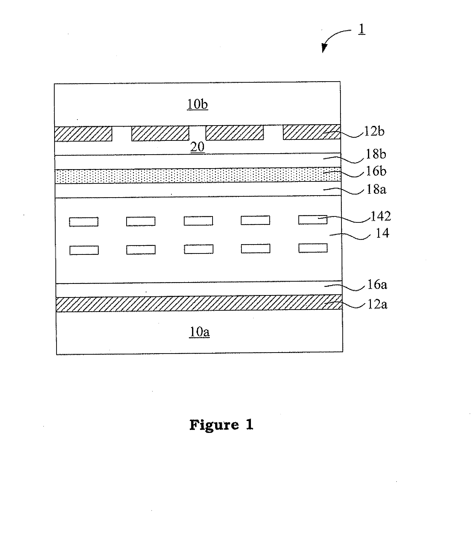
[0023]FIG. 1 illustrates a cross-section diagram for a controllable optical device disclosed by the invention. As shown in FIG. 1, the optical device 1 comprises a first substrate 10a, a first conductive layer 12a, a liquid crystal layer 14, a semiconductor layer 20, a second conductive layer 12b and a second substrate 10b. In the embodiment, the first conductive layer 12a is formed on the first substrate 10a, the liquid crystal layer 14 is formed on the first conductive layer 12a, the semiconductor layer 20 is formed on the liquid crystal layer 14, the second conductive layer 12b is formed on the semiconductor layer 20, and the second substrate 10b is formed on the second conductive layer 12b. Wherein, the first conductive layer 12a and the second conductive layer 12b are used as the control electrodes for the optical device 1 with controllable voltage, all are transparent conductive layers. The Indium Tin Oxide (ITO) is often used as the material of transparent conductive layer. T...


PUM


Abstract

A controllable optical device comprises a first substrate, a first conductive layer, a liquid crystal layer, a semiconductor conductive layer, a second conductive layer, and a second substrate. The first conductive layer is formed on the first substrate, the liquid crystal layer is formed on the first conductive layer, the semiconductor conductive layer is formed on the liquid crystal layer, the second conductive layer is formed on the semiconductor layer, and the second substrate is formed on the second conductive layer.

Description

BACKGROUND OF THE INVENTION[0001]1. Field of the Invention[0002]The invention relates to an optical device, particularly to a controllable optical device.[0003]2. Description of the Prior Art[0004]The liquid crystal lens or liquid lens is composed of liquid crystal polymer mixture or oil and water mixture. The arrangement of these fluids will be changed in accordance with the change of electrical field distribution. This property is utilized by the optical device to focus or diverge the light beam.[0005]The conventional optical focus-changing lens set needs at least two lenses to obtain the focus-changing effect. The shortcoming of the method is that it is heavier and larger than current optical focus-changing lens set.[0006]In addition, in order to obtain the required phase retardation effect, the liquid crystal lens usually needs thicker liquid crystal layer. However, thicker liquid crystal layer will cause longer response time. For example, if the liquid crystal layer is 60 μm th...

Claims


Application Information

Patent Timeline
IPC IPC(8): G02B3/12
CPCG02B3/14G02B3/12
Inventor LIU, LI-WEICHEN, CHIH-WEISU, YONG-RENHUANG, YI-PAI
Owner NATIONAL CHIAO TUNG UNIVERSITY
Why Eureka
Try Eureka