Optical semiconductor based illuminating apparatus

a technology of optical semiconductors and illuminating devices, applied in lighting and heating devices, lighting support devices, light source combinations, etc., can solve the problems of large heat generation of illuminating devices, poor appearance of heat sinks, and inability to disassemble and reassemble the entire illuminating apparatus, etc., to achieve simple separation and fastening, excellent waterproofing characteristics and durability, and promote convenience for checking and repairing

Inactive Publication Date: 2013-04-11
POSCO LED
View PDF17 Cites 30 Cited by
  • Summary
  • Abstract
  • Description
  • Claims
  • Application Information

AI Technical Summary

Benefits of technology

[0014]The present invention provides an optical semiconductor based illuminating apparatus capable of promoting convenience for checking and repairing, simply ...

Problems solved by technology

In the case in which a plurality of products are embedded in the illuminating apparatus, when a fault occurs in each product, the entire illuminating apparatus cannot but be disassembled and reassembled.
However, the heat sink is polluted by excrement of birds that tend to sit down at a high place, such that the heat...

Method used


Image

  • Optical semiconductor based illuminating apparatus
  • Optical semiconductor based illuminating apparatus
  • Optical semiconductor based illuminating apparatus

Examples


Embodiment Construction

[0094]Hereinafter, exemplary embodiments of the present invention will be described in detail with reference to the accompanying drawings.

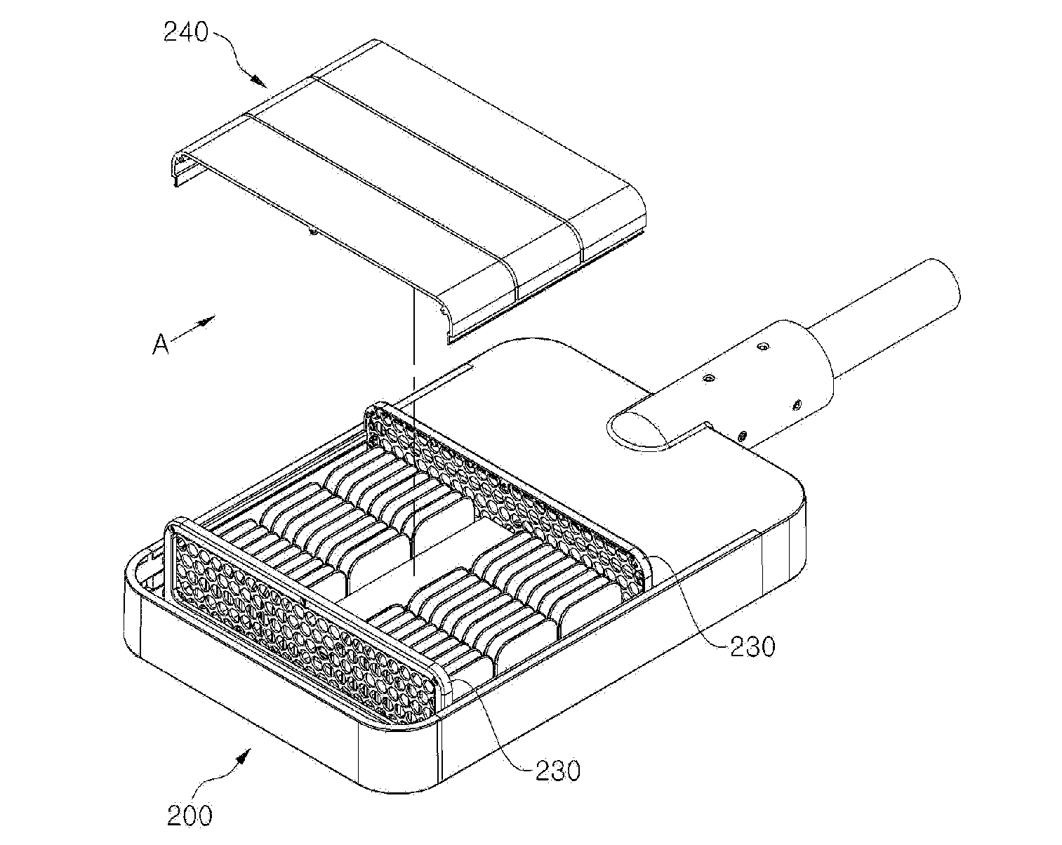
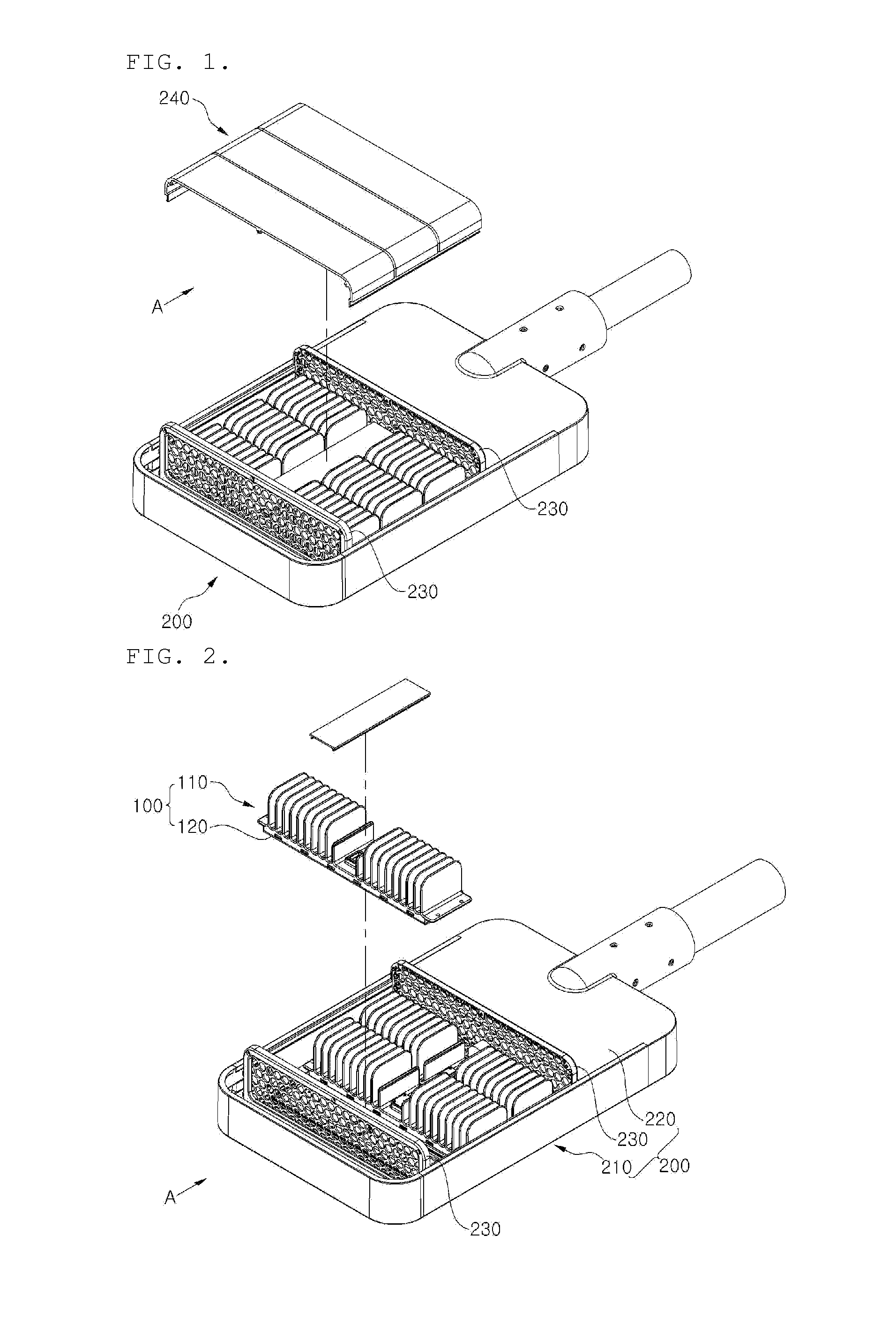
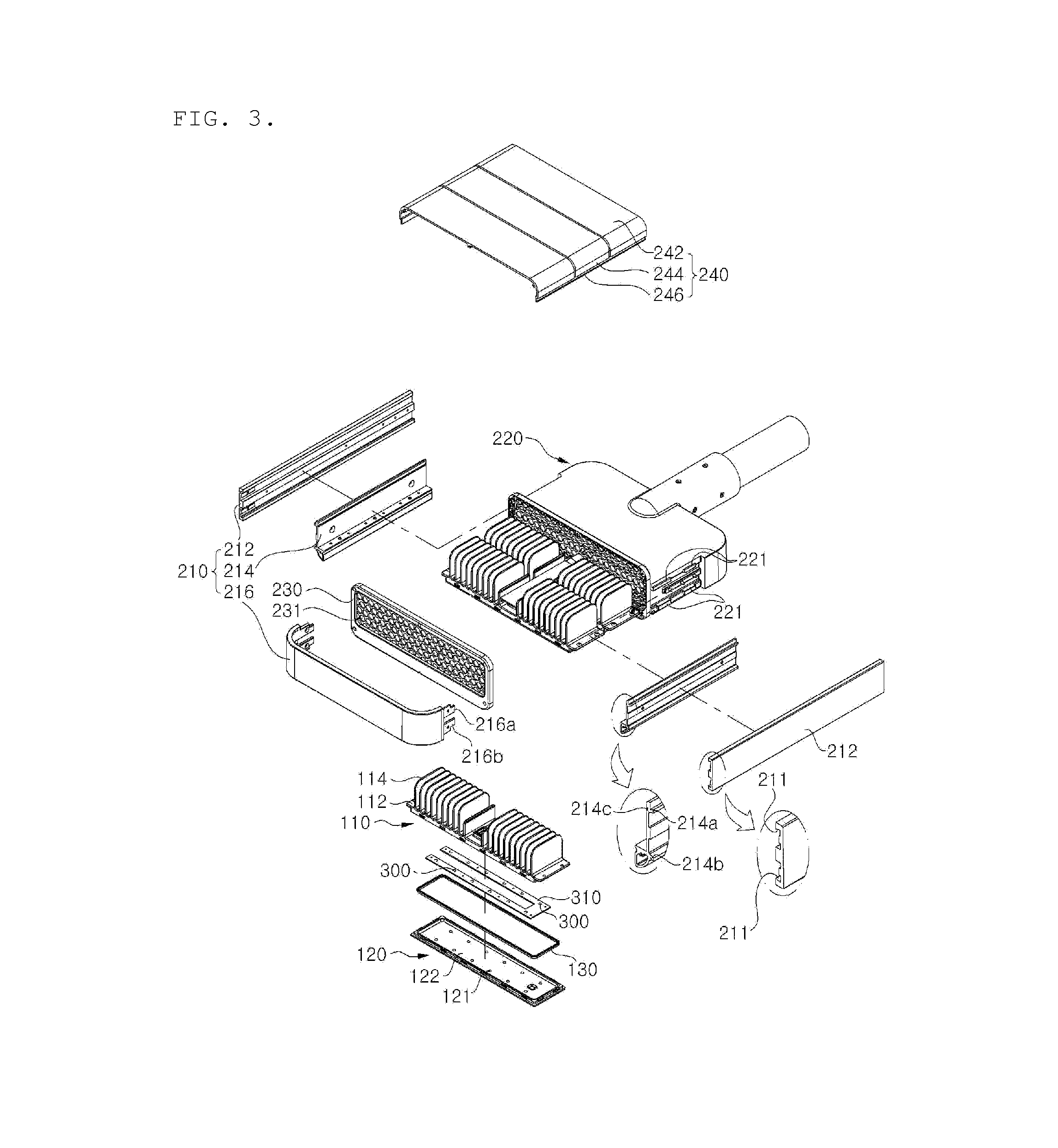
[0095]FIGS. 1 and 2 are perspective views showing a process of separating an optical semiconductor based illuminating apparatus according to an exemplary embodiment of the present invention; FIG. 3 is an exploded perspective view showing the entire configuration of the optical semiconductor based illuminating apparatus according to the exemplary embodiment of the present invention; and FIG. 4 is a partially cut-away perspective view showing a coupling relationship between a light emitting module and a housing which are main parts of the optical semiconductor based illuminating apparatus according to the exemplary embodiment of the present invention.

[0096]The optical semiconductor based illuminating apparatus according to the present invention may includes a housing 200 mounted with at least one light emitting module 100 including a semiconductor o...


PUM


Abstract

Disclosed herein is an optical semiconductor based illuminating apparatus including light emitting modules including at least one semiconductor optical device; and a housing enclosing one side surface of at least one of the light emitting modules. This optical semiconductor based illuminating apparatus may promote convenience for checking and repairing, simply perform separation and fastening, have excellent waterproofing characteristics and durability, prevent accidents such as short circuit and electric shock improve heat radiation performance, prevent introduction of foreign materials, be easily cleaned and maintained, reliably provide power of a main power line to a plurality of light emitting modules, and utilize a space and secure reliability of a product regardless of a size and a shape of a power supply embedded therein.

Description

CROSS-REFERENCE TO RELATED APPLICATIONS[0001]This application claims priority from and the benefit of Korean Patent Application No. 2011-0103259, filed on Oct. 10, 2011, Korean Patent Application No. 2011-0108062, filed on Oct. 21, 2011, and Korean Patent Application No. 2011-0116739, filed on Nov. 10, 2011, which is hereby incorporated by reference for all purposes as if fully set forth herein.BACKGROUND OF THE INVENTION[0002]1. Field of the Invention[0003]The present invention relates to an optical semiconductor based illuminating apparatus.[0004]2. Discussion of the Background[0005]An optical semiconductor such as a light emitting diode (LED) is one of the components that have been recently spotlighted widely as an illuminating apparatus since it has lower power consumption, a longer lifespan, more excellent durability, and significantly higher brightness as compared with an incandescent lamp and a fluorescent lamp.[0006]Particularly, an illuminating apparatus using the optical s...

Claims


Application Information

Patent Timeline
IPC IPC(8): F21V29/00F21V21/00
CPCF21V29/004F21V15/01F21V3/00F21S2/005F21V19/04F21V23/001F21V23/02F21V23/06F21W2131/103F21Y2101/02F21Y2105/001F21V29/006F21V29/2212F21V29/507F21V29/763F21V29/83F21V31/03F21Y2105/10F21Y2115/10F21Y2113/00F21V29/76F21V29/60F21V29/717
Inventor YUN, KYUNG MINKIM, SEUNG KILEE, SU WOON
Owner POSCO LED
Why Eureka
Try Eureka