Printed circuit board capable of limiting electromagnetic interference

Inactive Publication Date: 2013-04-18
HON HAI PRECISION IND CO LTD
View PDF72 Cites 1 Cited by
  • Summary
  • Abstract
  • Description
  • Claims
  • Application Information

AI Technical Summary

Benefits of technology

The present patent relates to a printed circuit board (PCB) that can limit electromagnetic interference (EMI) produced by itself. The PCB includes a first wiring layer that produces EMI, a power layer, a grounded layer, and a second wiring layer. The PCB also includes dielectric layers placed between the layers. The PCB has a first portion of the power layer that is isolated from the power layer to form an independent power area (IPA) that provides power to the interference source. The PCB can reduce interference and improve the performance of electronic devices that use it.

Problems solved by technology

The timed signals would be converted to frequency domain signals, however, the frequency domain signals may be interference frequency to the PCB 1, therefore, the time schedule controller is a source of interference on the PCB 1.

Method used


Image

  • Printed circuit board capable of limiting electromagnetic interference
  • Printed circuit board capable of limiting electromagnetic interference
  • Printed circuit board capable of limiting electromagnetic interference

Examples


Embodiment Construction

[0010]Embodiments of the present disclosure will be described, with reference to the accompanying drawings.

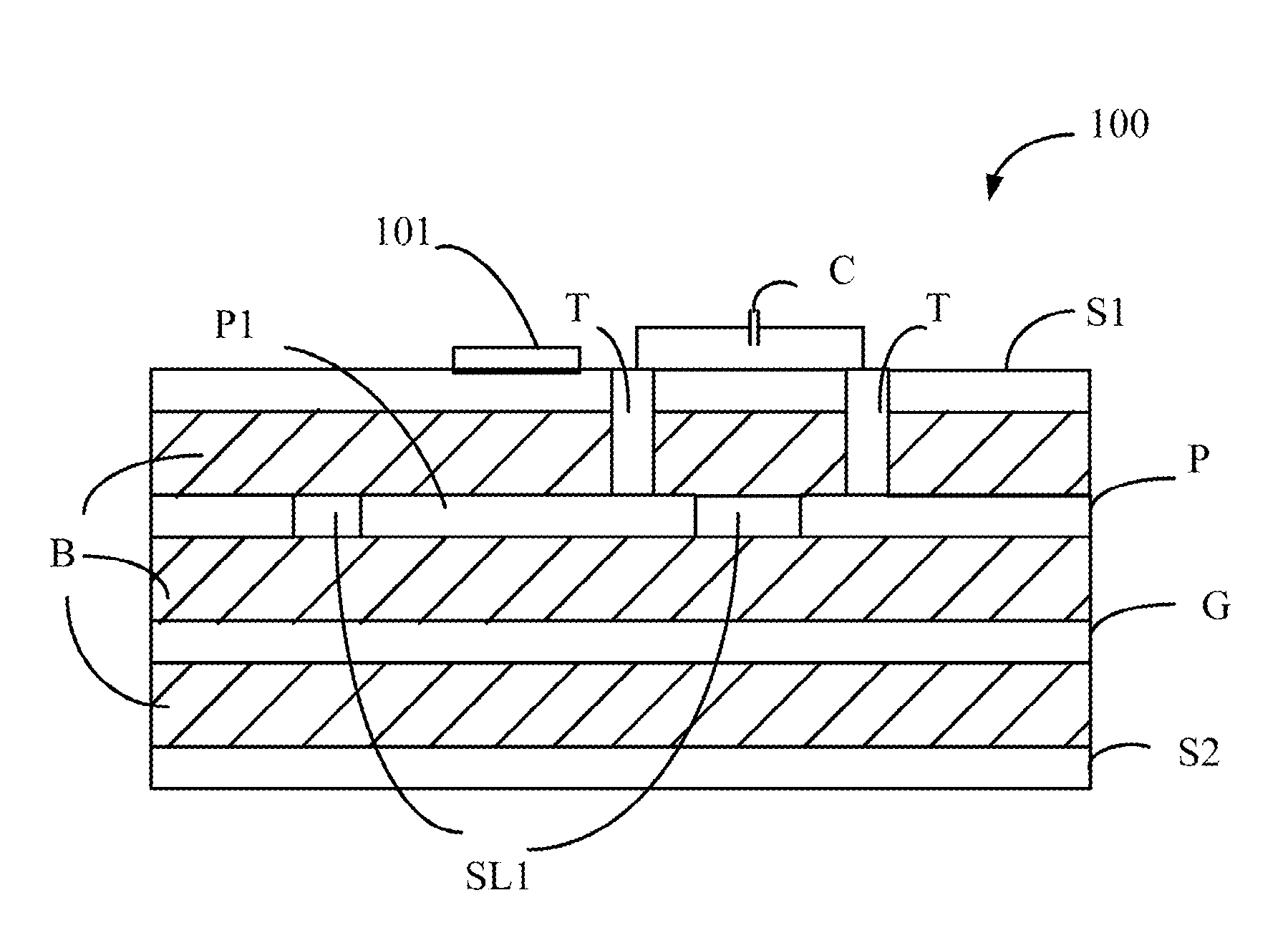
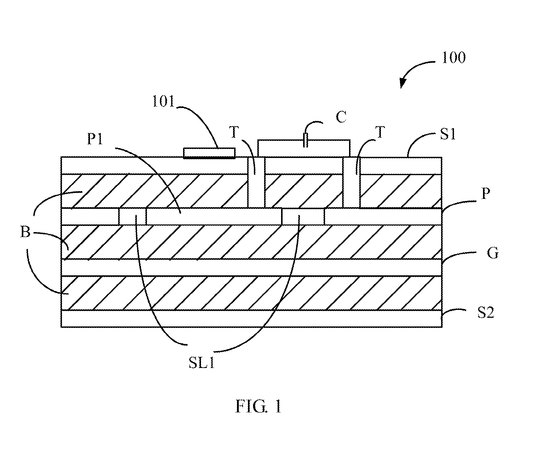
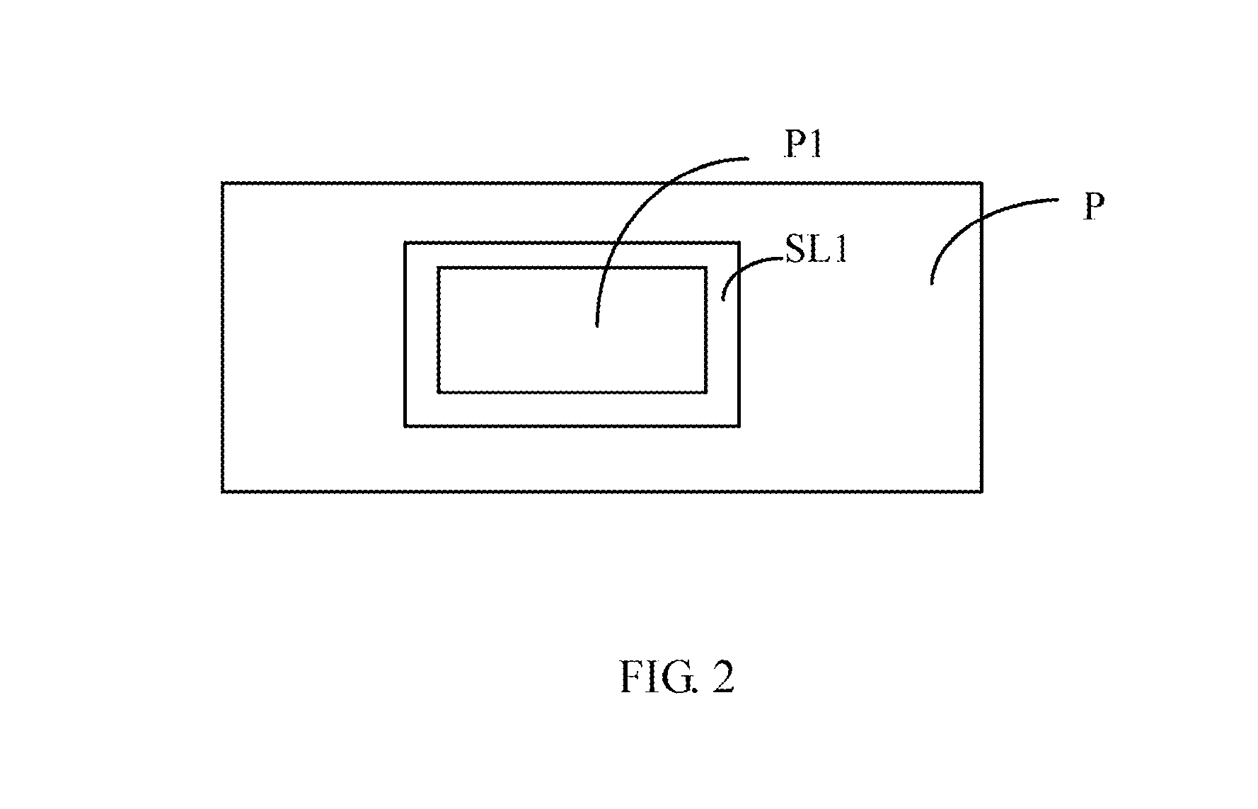
[0011]Referring to FIGS. 1 and 2 together, a printed circuit board (PCB) 100 capable of limiting electromagnetic interference produced by itself is shown. The PCB 100 includes a first wiring layer S1, a power layer P, a grounded layer G, and a second wiring layer S2. The PCB 100 also includes dielectric layers B which are placed between each adjacent two layers of the first wiring layer S1, the power layer P, the grounded layer G, and the second wiring layer S2. The power layer P is used to provide power to the first wiring layer S1 and to the second wiring layer S2, the grounded layer G is used to provide a ground connection to the first wiring layer S1 and to the second wiring layer S2.

[0012]The first wiring layer S1 includes an interference source 101 which produces electromagnetic interference, in the embodiment, the interference source 101 is a time schedule controller. A ...


PUM


Abstract

A printed circuit board (PCB) includes a first wiring layer, a second wring layer, a power layer, a grounded layer, dielectric layers between every two active layers, a capacitor, and two through holes. A first portion of the power layer corresponding to the electromagnetic interference source is isolated from the power layer to form an independent power area. A first through hole connects the independent power area to an end of the capacitor, the second through hole connects a second portion of the power area to the other end of the capacitor. When the interference source produces interference, the interference is conducted to the independent power area and conducted to the second portion of the power area via the through holes and the capacitor.

Description

TECHNICAL FIELD[0001]The present disclosure relates to printed circuit boards, particularly, to a printed circuit board capable of limiting electromagnetic interface produced by itself.DESCRIPTION OF RELATED ART[0002]Many printed circuit boards (PCBs) include multiple layers. For example, a PCB 1 including four layers is shown in FIG. 5, the PCB 1 includes a first wiring layer Si, a power layer P, a grounded layer G, and a second wiring layer S2 which are arranged in sequence. Therein, there is a dielectric layer B placed between each two adjacent layers of the first wiring layer S1, the power layer P, the grounded layer G, and the second wiring layer S2. The power layer P is used to provide power to the first wiring layer S1 and to the second wiring layer S2, the grounded layer G is used to provide a ground connection to the first wiring layer S1 and to the second wiring layer S2. The first wiring layer S1 may include a time schedule controller used to produce timed signals on a sc...

Claims


Application Information

Patent Timeline
IPC IPC(8): H05K1/16
CPCH05K1/0225H05K1/0227H05K2201/10015H05K2201/09972H05K1/0243
Inventor WANG, CHENG-SUNG
Owner HON HAI PRECISION IND CO LTD
Why Eureka
Try Eureka