Low-EMI electronic apparatus, low-EMI circuit board, and method of manufacturing the low-EMI circuit board

a technology of electronic equipment and circuit boards, which is applied in the direction of sustainable manufacturing/processing, final product manufacturing, printed circuit non-printed electric components association, etc., can solve the problems of increasing the cost of electronic equipment. , to achieve the effect of reducing the cost, reducing the cost, and suppressing the spurious radiation

Inactive Publication Date: 2002-02-07
SUMITOMO RUBBER IND LTD
View PDF0 Cites 74 Cited by
  • Summary
  • Abstract
  • Description
  • Claims
  • Application Information

AI Technical Summary

Benefits of technology

0038] The present invention aims to suppress the spurious radiation at the level of the circuit board, and it eliminates various countermeasure parts such as a common mode choke, a filter and a bypass capacitor for an I/O unit and a power code which have been required in the prior art, and solves the problems of {circle over (1)} the increase of cost of the electronic apparatus, {circle over (2)} problems to so-called high packaging density such as minituarization, thinning and weight reduction of the product due to the increase of volume, {circle over (3)} the complexity of the countermeasure parts, and {circle over ...

Problems solved by technology

Recently, the rise of an operating frequency due to high performance of a product raises a radiation intensity of spurious radiation, which leads the EMI to a severe situation.
Further, with the population of the electronic products, the countermeasure for the EMI of the electronic products is becoming severer.
If the spurious radiation increases in this manner, the electromagnetic environment becomes more and more worse and it is no doubt that a television video screen is disturbed or a manipulation system of an aircraft becomes uncontrollable and social problems are raised.
In order to enhance the EMC performance of the product, various countermeasure parts such as a common mode choke, a filter and a bypass capacitor for an I/O unit and a power supply have been used from the past but these parts present demerits of {circle over (1)} increase of a cost, {circle over (2)} problem to so-called high packaging density such as minituarization, thinning and weight reduction of a product due to the increase of volume, {circle over (3)} complexity of the countermeasure part, and {circle over (4)} restriction to external view design.
Further, in such a prior art product, the conformity to the f...

Method used


Image

  • Low-EMI electronic apparatus, low-EMI circuit board, and method of manufacturing the low-EMI circuit board
  • Low-EMI electronic apparatus, low-EMI circuit board, and method of manufacturing the low-EMI circuit board
  • Low-EMI electronic apparatus, low-EMI circuit board, and method of manufacturing the low-EMI circuit board

Examples


Embodiment Construction

[0123] The embodiments of the present invention are now explained.

[0124] FIG. 33 shows an external view of an electronic apparatus (personal computer) using a low EMI circuit board in accordance with one embodiment of the present invention.

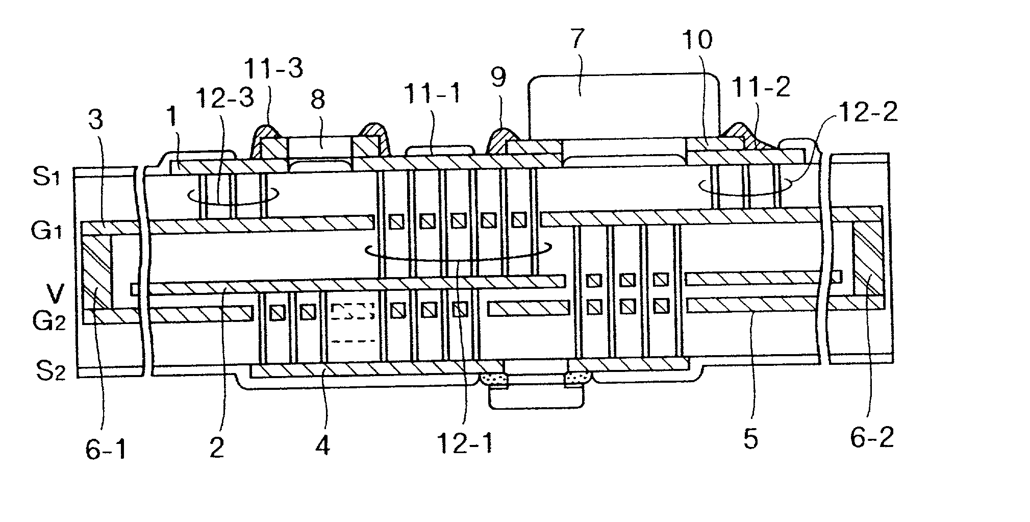
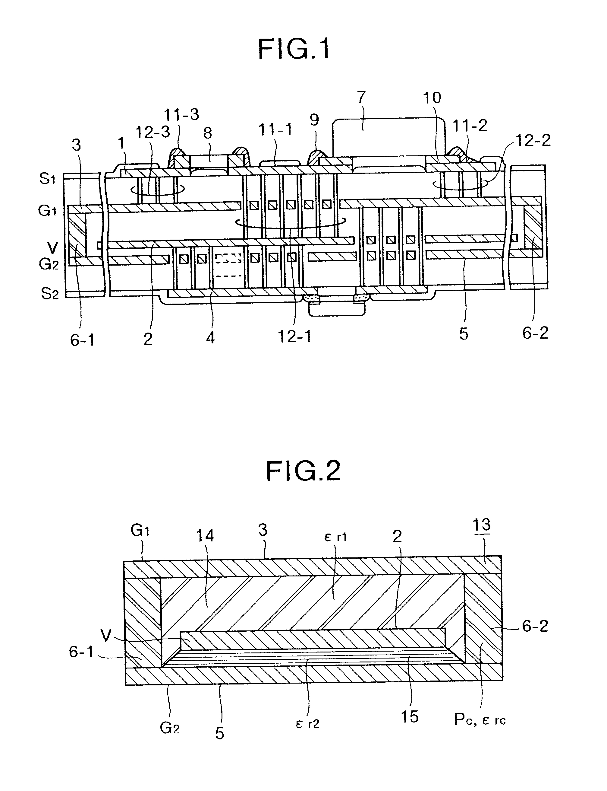
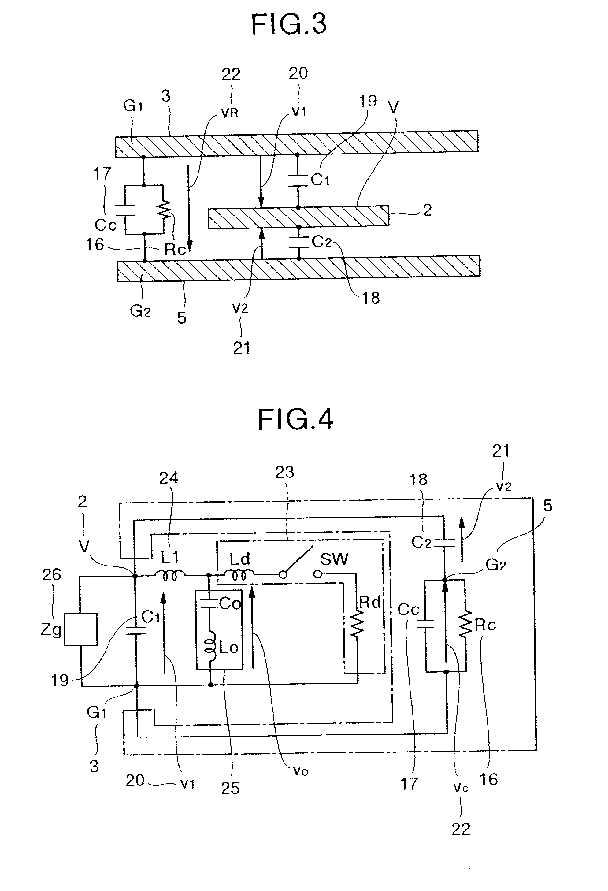
[0125] In the electronic apparatus 1 of the present invention, components comprising I / O connectors 4 (4-1, . . . , 4-5), a power code 5, a signal cable 6, a housing 7, an LCD display 8, a keyboard 9, a floppy disk drive 10, a hard disk drive 11, a battery pack 12 and an IC card 13 are electrically and physically connected around a low EMI circuit board 3 on which a high speed CPU 2 is mounted. The low EMI circuit board 3 comprises "first and second ground layers having at least one thereof electrically connected to electrical parts, a power layer provided between said first ground layer and said second ground layer and electrically connected to said electronic parts, a dielectric material layer for joining said second ground layer and said power ...


PUM

PropertyMeasurementUnit
Dielectric polarization enthalpyaaaaaaaaaa
Densityaaaaaaaaaa
Shapeaaaaaaaaaa

Abstract

A low-EMI circuit which realizes a high mounting density by converting the potential fluctuation of a power supply layer with respect to a ground layer which occurs on switching an IC device etc., into Joule's heat in the substrate without using any parts as a countermeasure against the EMI. Its structure, a circuit board using it, and a method of manufacturing the circuit board are also disclosed. Parallel plate lines in which the Q-value of the stray capacitance between solid layers viewed from the power supply layer and ground layer is equivalently reduced and which are matchedly terminated by forming a structure in which a resistor (resistor layer) and another ground layer are provided in addition to the power supply layer and the ground layer on a multilayered circuit board. A closed shield structure is also disclosed. This invention can remarkably suppress unwanted radiation by absorbing the potential fluctuation (resonance) which occurs in a power supply loop by equivalently reducing the Q-value of the stray capacitance, absorbing the standing wave by the parallel plate lines matchedly terminated and, closing and shielding the parallel plate lines.

Description

[0001] This is a continuation application of U.S. application Ser. No. 08 / 860,181, filed Jul. 10, 1997, which is a 371 filing of PCT / JP96 / 00021, filed on Jan. 10, 1996, and the entire disclosures of which are incorporated herein by reference.[0002] The present invention relates to an electronic apparatus which copes with an EMC which is becoming more and more important in increasing speed and packaging density of IC and LSI devices, and to a device, a circuit board and an electronic apparatus which require suppression means for spurious radiation noise and a method of making the same.[0003] An EMC intends to the compatibility of an electromagnetic environment of an EMI (noise source) and an immunity (noise receiver). Recently, the rise of an operating frequency due to high performance of a product raises a radiation intensity of spurious radiation, which leads the EMI to a severe situation. Further, with the population of the electronic products, the countermeasure for the EMI of th...

Claims


Application Information

Patent Timeline
IPC IPC(8): H01L23/538H01L23/552H01L25/16H05K1/02H05K1/09H05K1/11H05K1/16H05K3/40H05K3/42H05K3/46H05K9/00
CPCH01L23/5383Y10T29/49155H01L25/16H01L2224/16H01L2924/01046H01L2924/01057H01L2924/01078H01L2924/01079H01L2924/09701H01L2924/16152H01L2924/19105H01L2924/19106H01L2924/3011H01L2924/3025H05K1/0227H05K1/0231H05K1/0234H05K1/0246H05K1/092H05K1/113H05K1/115H05K1/162H05K1/167H05K3/403H05K3/4053H05K3/429H05K3/4611H05K3/4614H05K3/4652H05K3/467H05K9/0039H05K2201/0209H05K2201/0715H05K2201/093H05K2201/09309H05K2201/09354H05K2201/09509H05K2201/09518H05K2201/09563H05K2201/09663H05K2201/0979H05K2201/10022H05K2201/10045H05K2201/10446H05K2201/10636H05K2201/10689H01L2924/01019H01L23/552H01L2924/00014Y02P70/50H01L2224/0401H05K3/46
Inventor AKIBA, YUTAKANARIZUKA, YASUNORITANEI, HIRAYOSHIKITAMURA, NAOYA
Owner SUMITOMO RUBBER IND LTD
Why Eureka
Try Eureka