Inclusion of chip elements in a sheathed wire

a technology of chip elements and sheathed wires, applied in the field of microelectronic chip elements, can solve problems such as handling problems, and achieve the effect of small siz

Active Publication Date: 2013-04-18
COMMISSARIAT A LENERGIE ATOMIQUE ET AUX ENERGIES ALTERNATIVES
View PDF3 Cites 30 Cited by
  • Summary
  • Abstract
  • Description
  • Claims
  • Application Information

AI Technical Summary

Benefits of technology

[0006]Thus, a solution for easing the handling of individualized chip elements of very small size is needed, especially when said elements are provided with wire sections which are desired to be kept substantially rectilinear.

Problems solved by technology

Once formed, such devices are to be incorporated in the objects to be identified, This poses handling problems, since the antennas should remain substantially rectilinear, or should at least not be shorted by twisting.

Method used


Image

  • Inclusion of chip elements in a sheathed wire
  • Inclusion of chip elements in a sheathed wire
  • Inclusion of chip elements in a sheathed wire

Examples


Embodiment Construction

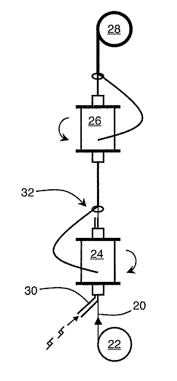
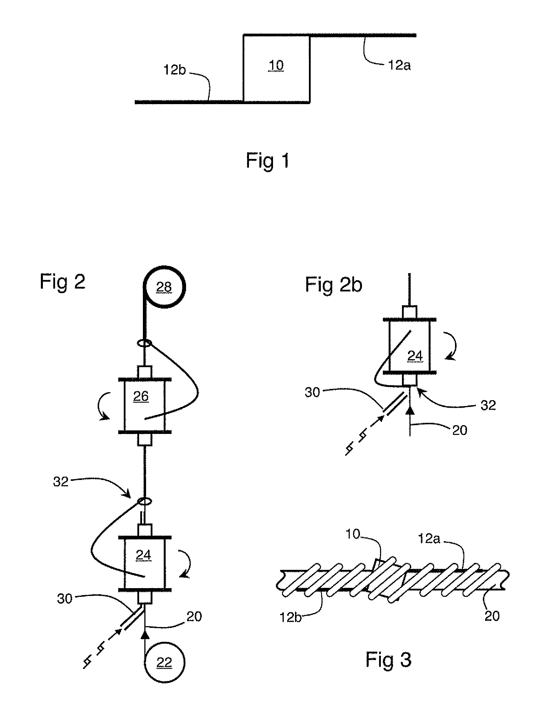
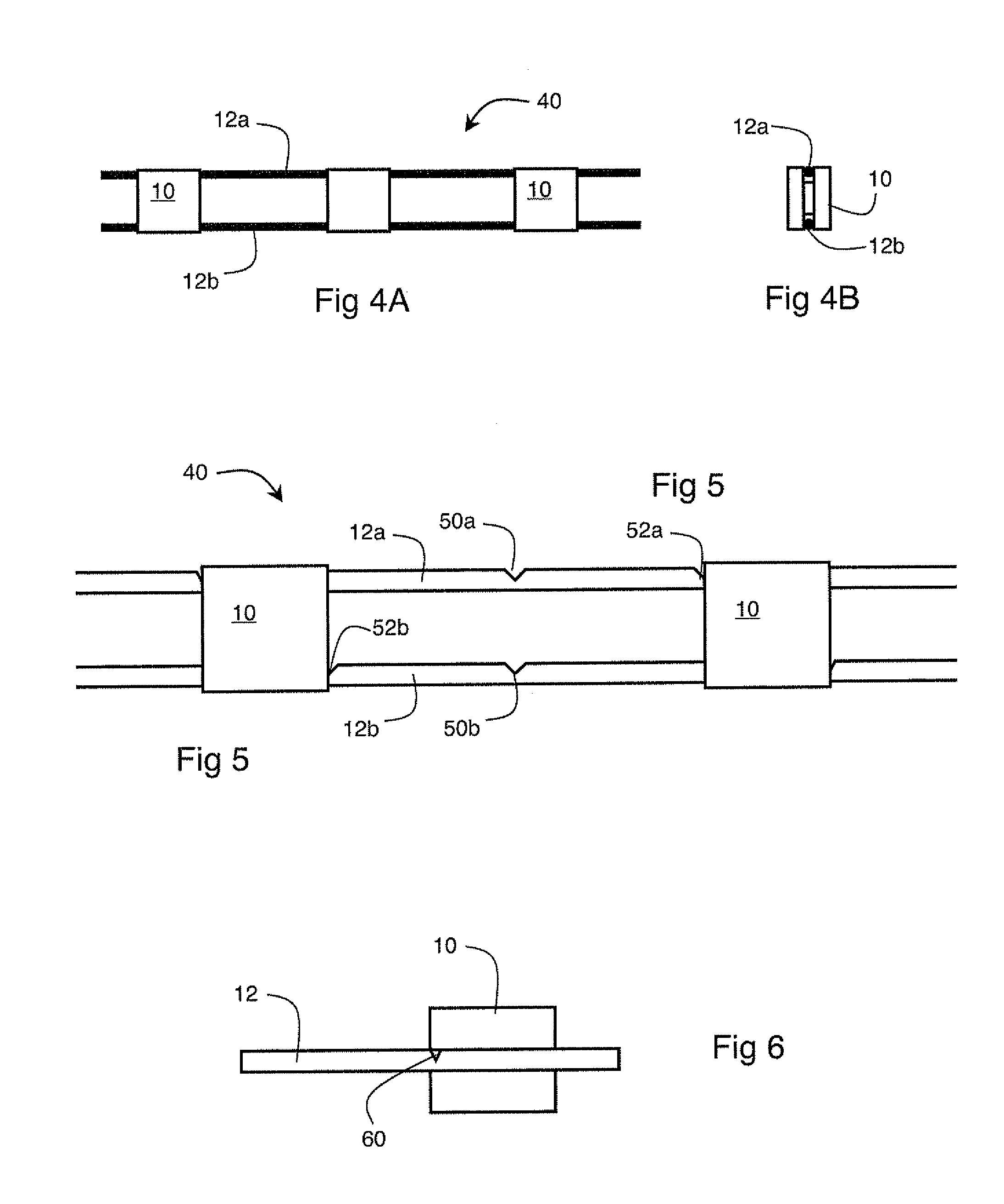
[0018]To ease the handling of individualized chip elements of very small size (possibly smaller than 1 mm), it is provided to incorporate them in spaced-apart fashion in a sheathed wire. The chip elements will be caught between the wire core and a sheathing fiber helically wrapped around the core.

[0019]To avoid for the chip elements to have the tendency to escape between the consecutive spirals of the sheathing fiber, said elements will be provided with wire sections also caught between the core and the sheathing fiber. The sheathing sections may advantageously be the dipole antennas of chip elements integrating radio frequency transmit-receive functions, or RFID.

[0020]The sheathed wire, wrapped on a spool, can be easy manipulated. In addition to the fact that the wire may be used to manufacture fabrics, it may be cut and incorporated in other objects, manually or in automated fashion, by limiting risks of losing the chip elements or of twisting the dipole antennas.

[0021]FIG. 2 sche...


PUM

PropertyMeasurementUnit
sizeaaaaaaaaaa
tensile stressaaaaaaaaaa
frictionaaaaaaaaaa

Abstract

A method for forming a sheathed wire includes the steps of axially advancing a core through a sheathing zone; wrapping a sheathing fiber around the core in the sheathing zone; and providing, in the sheathing zone, a series of microelectronic chip elements each provided with a wire section, in such a way that the sheathing fiber that wraps around the core also wraps around a chip element and the wire section thereof to form a sheathed wire incorporating spaced-apart chip elements.

Description

BACKGROUND OF THE INVENTION[0001]The invention relates to microelectronic chip elements having a largest dimension that may be smaller than one millimeter. The invention more specifically relates to a method for packaging such chip elements to ease their storage and their manipulation.STATE OF THE ART[0002]FIG. 1 schematically shows a miniaturized radio frequency transceiver device, for example used for contactless identification (RFID-type device). The device comprises a chip element 10, of generally parallelepipedal shape, incorporating a chip which integrates all RFID functions.[0003]The device comprises a dipole antenna formed of two conductor wire sections 12a and 12b. These sections, connected to two opposite surfaces of element 10, are connected to terminals of the chip and extend in opposite directions.[0004]Since the large side of chip element 10 may be shorter than 1 mm, these devices are not manufactured and manipulated by methods used for larger devices.[0005]Patent appl...

Claims


Application Information

Patent Timeline
Patent Type & Authority Applications(United States)
IPC IPC(8): G06K19/077
CPCD02G3/362Y10T29/49002G06K19/07718G06K19/07749G06K19/07758H01L24/78H01L24/85H01L25/0655H01L25/50H01L2224/78H01L2224/8517H01L2924/01014H01L2924/01058H01L2924/00014H01L2224/858D10B2401/18G06K19/07786H01L2224/48H01L2224/45099H01L2224/05599
Inventor BRUN, JEANLANCON, LAURENTVICARD, DOMINIQUE
Owner COMMISSARIAT A LENERGIE ATOMIQUE ET AUX ENERGIES ALTERNATIVES
Why Eureka
Try Eureka