Scanning probe microscopy-based metrology tool with a vacuum partition

a vacuum partition and scanning probe technology, applied in scanning probe techniques, instruments, coatings, etc., can solve the problem of sample exposed to contamination from microscope components

Inactive Publication Date: 2013-04-18
THE BOARD OF TRUSTEES OF THE LELAND STANFORD JUNIOR UNIV
View PDF17 Cites 8 Cited by
  • Summary
  • Abstract
  • Description
  • Claims
  • Application Information

AI Technical Summary

Benefits of technology

[0014]In another aspect of the invention, a pressure ratio exists between the first partition and the second partition, where the pressu

Problems solved by technology

Even the existing metrology tools that incorporate a vacuum environment do not separate the sample from

Method used


Image

  • Scanning probe microscopy-based metrology tool with a vacuum partition
  • Scanning probe microscopy-based metrology tool with a vacuum partition
  • Scanning probe microscopy-based metrology tool with a vacuum partition

Examples


Embodiment Construction

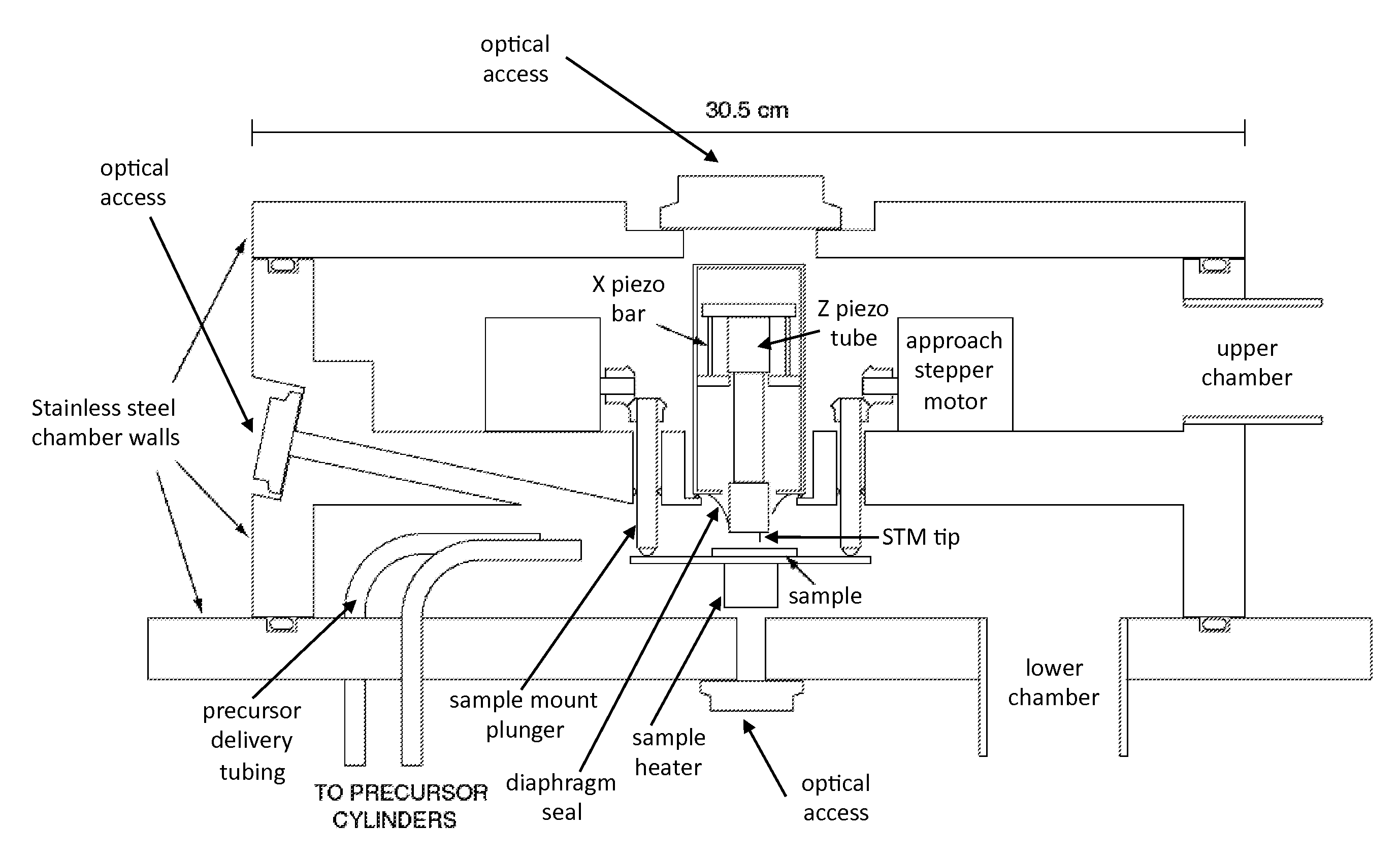
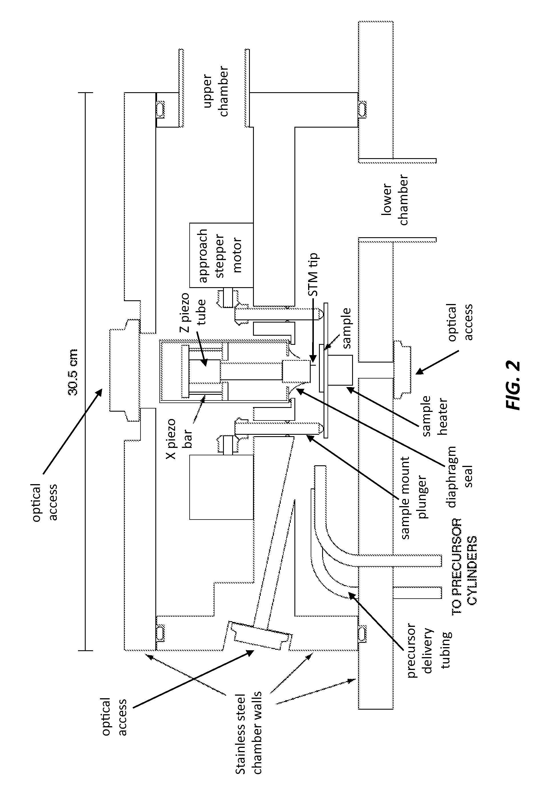
[0038]This invention is a metrology tool for semiconductor manufacturing. The tool incorporates a scanning probe microscope. The tool is partitioned so that the sample is not exposed to the microscope components, wherein the invention is used for metrology during semiconductor manufacturing. This partitioned configuration allows the tool to be mounted on a cluster tool for mid-process characterization. Mid-process characterization enables early detection of errors in processing, allowing defective wafers to be recycled or reprocessed. According to one embodiment, the mid-process characterization of wafers during semiconductor manufacturing enables determination of trench depth, material composition, feature height, feature spacing, size uniformity, capacitance, elastic modulus, and any other measurement that can be performed with a scanning probe microscope. Further, the invention enables mid-process characterization of micro-electromechanical systems (MEMS) and related devices to d...


PUM

PropertyMeasurementUnit
Pressureaaaaaaaaaa
Pressureaaaaaaaaaa
Densityaaaaaaaaaa

Abstract

A method of monitoring of semiconductor processes is provided that includes monitoring the processes using a scanning probe microscope (SPM), where a first partition is located below a second partition, where the second partition is hermetically isolated from the first partition, where a SPM probe tip of the SPM is disposed in the first partition, where a remaining portion of the SPM is disposed in the second partition that is hermetically isolated from the first partition, and where the semiconductor processes may occur in either the first partition or a third partition.

Description

CROSS-REFERENCE TO RELATED APPLICATIONS[0001]This application is a continuation-in-part of U.S. patent application Ser. No. 13 / 548,845 filed Jul. 13, 2012, which is incorporated herein by reference. U.S. patent application Ser. No. 13 / 548,845 is a continuation of U.S. patent application Ser. No. 12 / 383,467 filed Mar. 23, 2009, which is incorporated herein by reference. U.S. patent application Ser. No. 12 / 38346 claims the benefit from U.S. Provisional Application 61 / 070,636 filed Mar. 24, 2008, and which is hereby incorporated by reference.FIELD OF THE INVENTION[0002]The invention relates to relates to a device to inspect features on a sample during semiconductor manufacturing. More particularly the invention relates to a scanning probe microscope with a sample chamber that is separated from the microscope components by a partition.BACKGROUND OF THE INVENTION[0003]Many semiconductor processing techniques are designed to control materials at the nanoscale. Success of the process depen...

Claims


Application Information

Patent Timeline
IPC IPC(8): G01Q60/10
CPCG01Q60/10B82Y35/00C23C16/52C23C16/305C23C16/45525G01Q30/02
Inventor MACK, JAMES F.VAN STOCKUM, PHILIP B.YEMANE, YONAS T.PRINZ, FRIEDRICH B.
Owner THE BOARD OF TRUSTEES OF THE LELAND STANFORD JUNIOR UNIV
Why Eureka
Try Eureka