Protecting circuit and control circuit for reducing leakage current
- Summary
- Abstract
- Description
- Claims
- Application Information
AI Technical Summary
Benefits of technology
Problems solved by technology
Method used
Image
Examples
Embodiment Construction
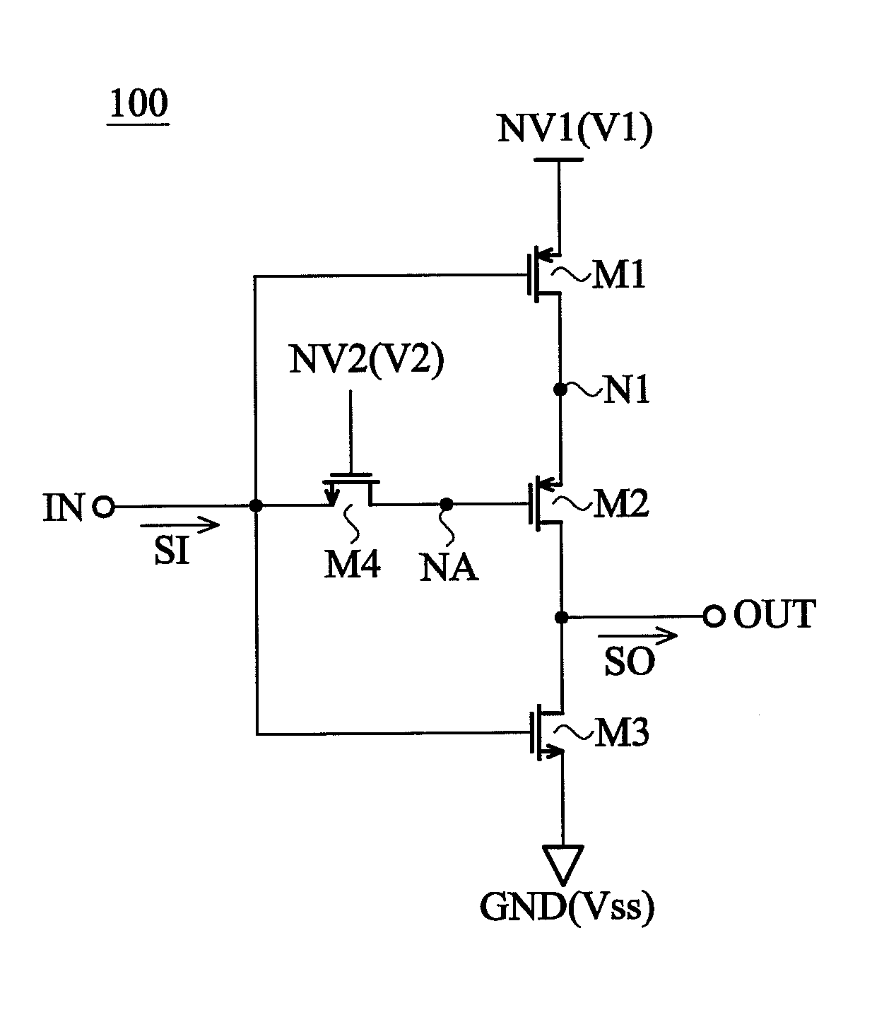
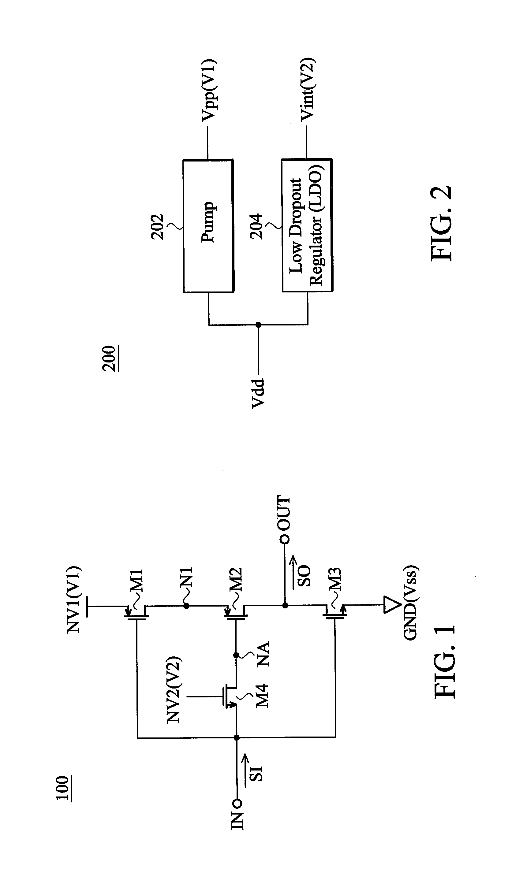
[0014]FIG. 1 is a diagram for illustrating a protecting circuit 100 according to an embodiment of the invention. As shown in FIG. 1, the protecting circuit 100 comprises PMOS transistors (P-channel Metal-Oxide-Semiconductor Field-Effect Transistor) M1, M2, and NMOS transistors (N-channel Metal-Oxide-Semiconductor Field-Effect Transistor) M3, M4. A ground node GND is configured to provide a ground voltage Vss. A first voltage node NV1 is configured to provide a first voltage V1, and a second voltage node NV2 is configured to provide a second voltage V2, wherein each of the first and second voltages V1, V2 is higher than the ground voltage Vss.
[0015]FIG. 2 is a diagram for illustrating a conversion circuit 200 according to an embodiment of the invention. As shown in FIG. 2, an external voltage Vdd (i.e., work voltage Vdd) of the protecting circuit is converted into a pump voltage Vpp through a pump 202 (i.e., a step-up circuit), and the external voltage Vdd is converted into an intern...
PUM
 Abstract
Description
Claims
Application Information


