Organic light-emitting panel, manufacturing method thereof, and organic display device

a technology of organic light-emitting panels and manufacturing methods, which is applied in the direction of electroluminescent light sources, thermoelectric devices, electric lighting sources, etc., can solve the problem of difficult uniform film thickness of the layer, and achieve excellent light-emitting characteristics, increase the inclination angle of the sidewall, and improve the effect of pinning location

Active Publication Date: 2013-05-02
JOLED INC
View PDF9 Cites 11 Cited by
  • Summary
  • Abstract
  • Description
  • Claims
  • Application Information

AI Technical Summary

Benefits of technology

[0012]The above organic light-emitting panel according to an aspect of the present invention is structured such that two inner sidewalls, which face each other in two adjacent banks defining the predetermined light-emitting cell, have different inclination angles. This structure makes it possible to adjust the pinning location when ink is dripped during the manufacturing. To be more specific, the larger the inclination angle of a sidewall of a bank is, the higher the pinning location is; and the smaller the inclination angle of a sidewall of a bank is, the lower the pinning location is.
[0013]Also, after the ink is dried, the film thickness of the organic light-emitting layer and the inclination angle of the bank sidewall have a reverse relationship. More specifically, the larger the inclination angle of a sidewall of a bank is, the smaller the film thickness of the organic light-emitting layer near the sidewall is, relatively; and the smaller the inclination angle of a sidewall of a bank is, the larger the film thickness of the organic light-emitting layer near the sidewall is, relatively.
[0014]Thus, with the structure where two inner sidewalls, which face each other in two adjacent banks defining the predetermined light-emitting cell, have different inclination angles, the organic light-emitting panel according to an aspect of the present invention can prevent the organic light-emitting layer in each light-emitting cell from becoming uneven in film thickness and provide excellent light-emitting characteristics.

Problems solved by technology

Meanwhile, a problem with the organic light-emitting layer formed in this way is that it is difficult for the layer to have a uniform film thickness.

Method used


Image

  • Organic light-emitting panel, manufacturing method thereof, and organic display device
  • Organic light-emitting panel, manufacturing method thereof, and organic display device
  • Organic light-emitting panel, manufacturing method thereof, and organic display device

Examples


embodiment 1

[0132]1. Configuration of Display Device 1

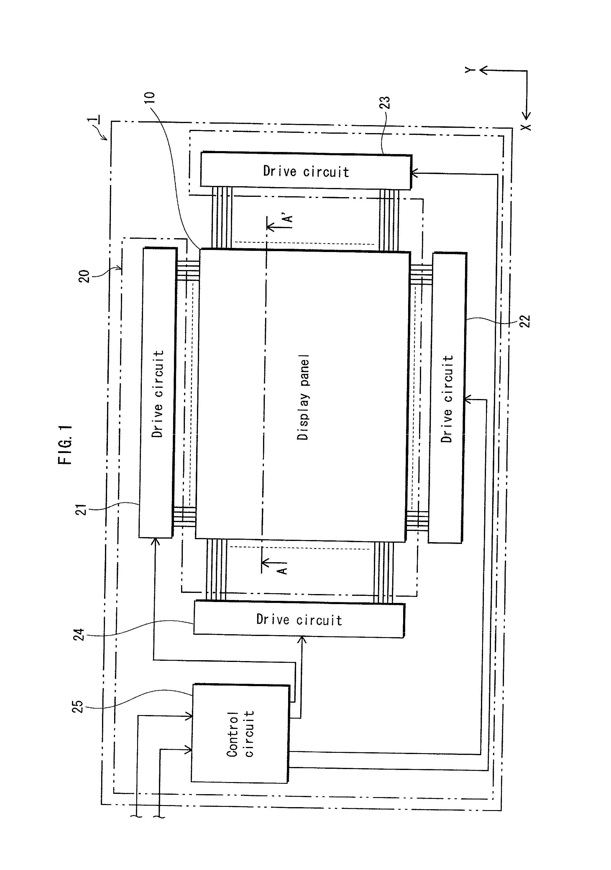
[0133]The overall structure of the display device 1 according to the present Embodiment is described with reference to FIG. 1.

[0134]As shown in FIG. 1, the display device (organic display device) 1 includes a display panel unit 10 and a drive control unit 20 connected to the display panel unit 10. The display panel unit 10 is an organic light-emitting panel that uses the phenomenon of electroluminescence occurring in organic material and is composed of a plurality of pixels arrayed two-dimensionally in the X-Y plane direction.

[0135]The drive control unit 20 is composed of four drive circuits 21-24 and a control circuit 25.

[0136]Note that in an actual display device 1, the placement of the drive control unit 20 with respect to the display panel unit 10 is not limited in this way.

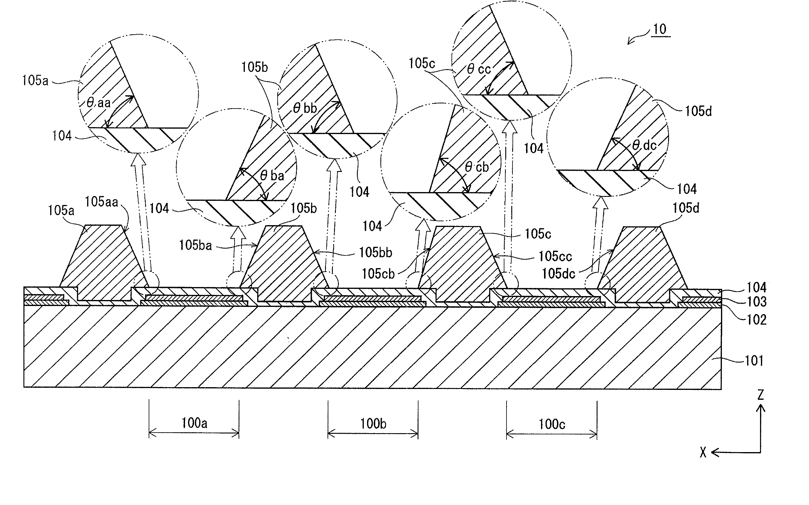
[0137]2. Structure of Display Panel 10

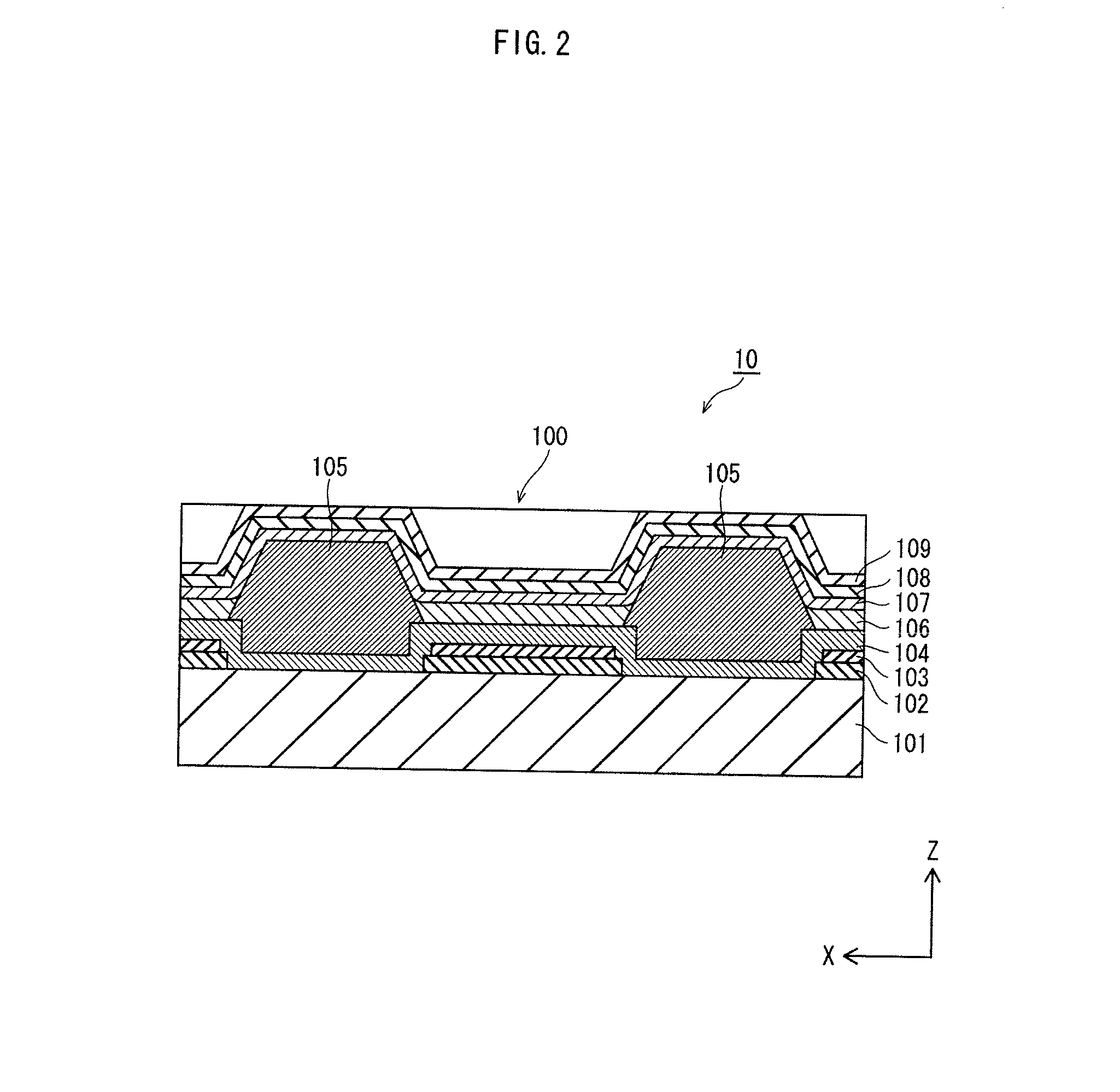
[0138]The structure of the display panel 10 is described with reference to FIG. 2. Note that, as an example, the display panel 1...

modification 1

[Modification 1]

[0210]Next, with reference to FIG. 13, Modification 1 of the manufacturing method of the display device 1 is described. FIG. 13 illustrates processes corresponding to processes illustrated in FIGS. 9C to 10A.

[0211]As shown in FIG. 13, first a bank material layer 1050 is formed to cover the hole injection transporting layer 104, and then a mask 503 is placed above the bank material layer 1050. The mask 503 is provided with light transmissive portions 503a, 503b, 503c1, 503c2, and 503d. The light transmissive portions 503a, 503b, 503c1, 503c2, and 503d are provided at locations corresponding to portions in which the banks 105a, 105b, 105c, and 105d are to be formed.

[0212]In the manufacturing method of the display device 1 in Modification 1, width Wa of the light transmissive portion 503a, which corresponds to the left-hand side of the planned sub-pixel formation region 1000a, is defined by points Pa1 and Pa2 at the feet of the sidewalls 105aa, . . . of the bank 105a (s...

modification 2

[Modification 2]

[0218]Next, with reference to FIGS. 14A to 15B, Modification 2 of the manufacturing method of the display device 1 is described. FIGS. 14A to 15B illustrate processes corresponding to the processes illustrated in FIGS. 9C to 10B.

[0219]As shown in FIG. 14A, first a bank material layer 1050 is formed to cover the hole injection transporting layer 104, and then a mask 504 is placed above the bank material layer 1050. The mask 504 has openings 504a, 504b, 504c, and 504d corresponding to the portions at which banks 105 are to be formed.

[0220]The openings 504a, 504b, and 504d are formed to have the same width as the opening 501a in the mask 501 used in the manufacturing method of the above Embodiment.

[0221]On the other hand, a width Wc3 of the opening 504c located between the planned sub-pixel formation regions 1000b and 1000d in correspondence with the bank 105c that is to be formed (see FIG. 4) is set to be larger than a width that is defined by points Pc3 and Pc2 being ...


PUM


Abstract

A pixel in the panel includes sub-pixels 100a, 100b, and 100c. Bank 105a separates organic light-emitting layer of sub-pixel 100a and organic light-emitting layer of a sub-pixel of a pixel that is adjacent to sub-pixel 100a. Bank 105d separates organic light-emitting layer of sub-pixel 100c and organic light-emitting layer of a sub-pixel of a pixel that is adjacent to sub-pixel 100c. Bank 105b separates organic light-emitting layer of sub-pixel 100a and organic light-emitting layer of sub-pixel 100b. Bank 105c separates organic light-emitting layer of sub-pixel 100b and organic light-emitting layer of sub-pixel 100c. Inclination angle θcb of sidewall 105cb of bank 105c located on the side of sub-pixel 100c is set to be larger than other inclination angles θaa, θba, θbb, θcc and θdc.

Description

[0001]This is a continuation application of PCT Application No. PCT / JP2010 / 006143 filed on Oct. 15, 2010, designating the United States of America, the disclosure of which, including the specification, drawings and claims, is incorporated herein by reference in its entirety.TECHNICAL FIELD[0002]The present invention relates an organic light-emitting panel, a manufacturing method thereof, and an organic display device.BACKGROUND ART[0003]In recent years, progress has been made in the research and development of display devices that use the phenomenon of electroluminescence occurring in organic material. Each light-emitting cell of such a display device is composed of an anode and a cathode with an organic light-emitting layer therebetween. When the display device is driven, holes are injected through the anode, electrons are injected through the cathode, and the holes and electrons recombine within the organic light-emitting layer, thereby emitting the light.[0004]Banks composed of i...

Claims


Application Information

Patent Timeline
Patent Type & Authority Applications(United States)
IPC IPC(8): H01L51/50H01L51/56H01L33/08H05B44/00
CPCH01L27/3211H01L27/3246H01L51/5228H01L51/0005H01L33/08H01L51/50H01L51/56H01L51/5234H10K59/35H10K71/135H10K59/122H10K50/824H10K50/828H10K50/00H10K71/00
Inventor MATSUSHIMA, HIDEAKI
Owner JOLED INC
Why Eureka
Try Eureka