Eureka AIR delivers breakthrough ideas for toughest innovation challenges, trusted by R&D personnel around the world.

Package structure and manufacturing method for the same

a packaging and manufacturing method technology, applied in the field of packaging structure, can solve the problems of thermal expansion and contraction, difficult to reduce the volume of the package, and pores inside the adhesive material

Inactive Publication Date: 2013-05-02
WALSIN LIHWA
View PDF6 Cites 13 Cited by
  • Summary
  • Abstract
  • Description
  • Claims
  • Application Information

AI Technical Summary

Benefits of technology

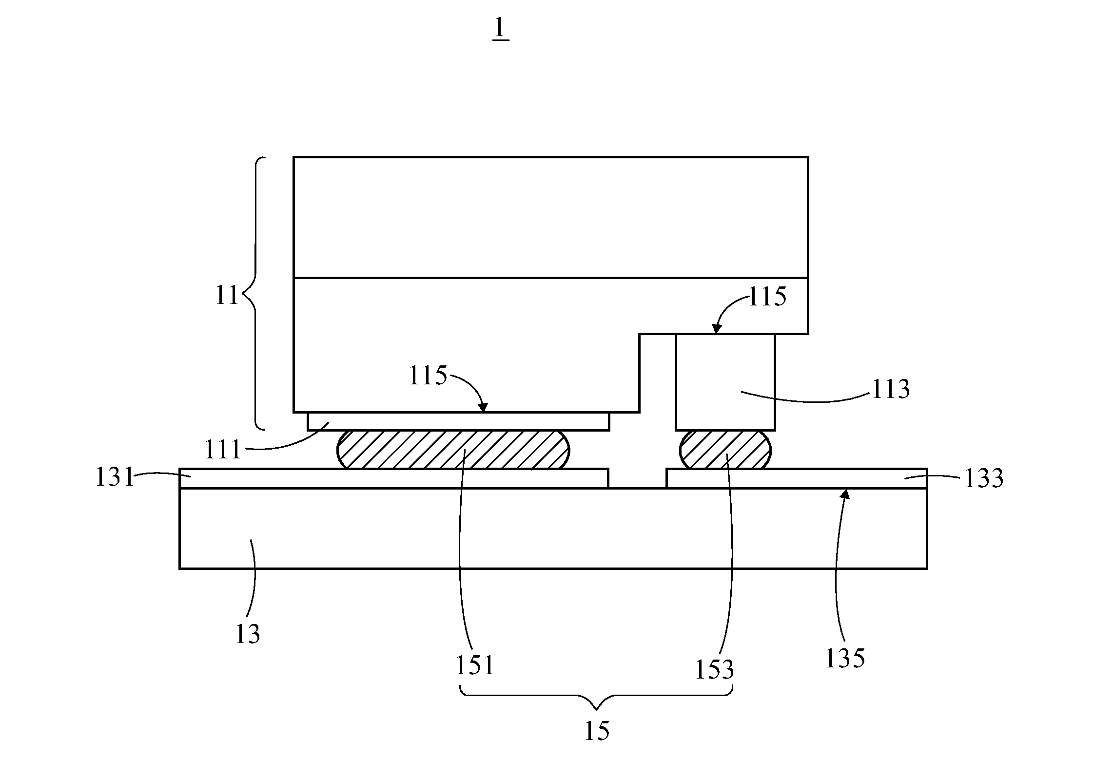
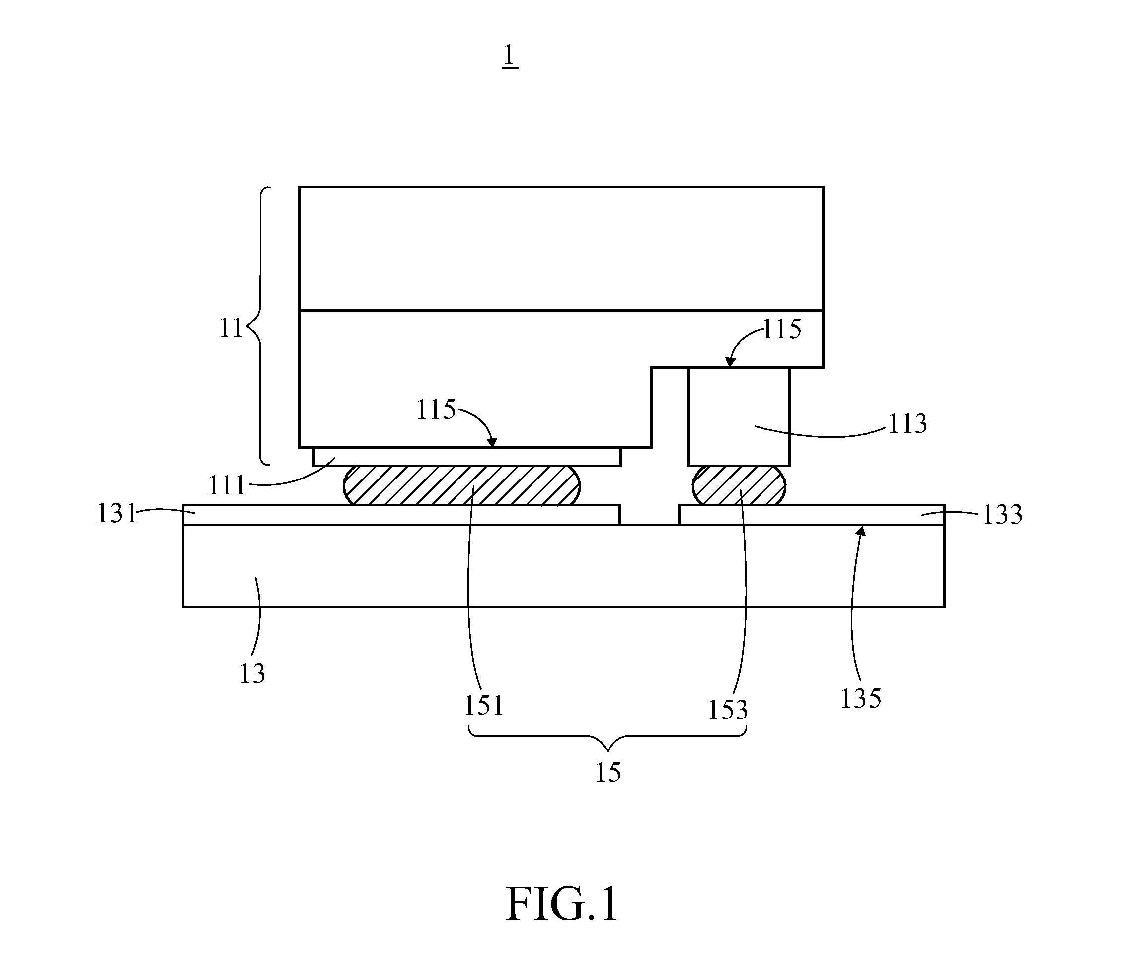
The present invention provides a package structure and a manufacturing method using a negative coefficient of thermal expansion (CTE) material for the electrical connection between the chip and the substrate. This helps to avoid alignment errors between the chip and the substrate that may affect signal transmission after curing the bonding material. The package structure includes a chip with electrode portions, a substrate with circuit portions, and an adhesive layer made of a metal compound with a negative CTE, which is placed between the electrode portions and the circuit portions to form an electrical connection. This adhesive layer helps to prevent shifting in the alignment between the chip and the substrate.

Problems solved by technology

However, both the conductive adhesives and the alloy solders used for adhering the chip to the substrate have properties of thermal expansion and contraction.
Therefore, when the temperature rises, the adhesive material will expand in volume to result in pores inside the adhesive material.
This not only makes it difficult to reduce the volume of the package by reducing the distance between the chip and the substrate, but may also enlarge the distance due to the presence of the pores, thus, causing alignment errors during the adhesion of the chip.
Moreover, when a metal solder is used in the chip adhering process, the high temperature of the melt alloy solder tends to cause damage to the insides of the chip and the substrate.
The high temperature may also cause stress changes in the chip and the substrate, which is unfavorable for subsequent manufacturing processes.

Method used


Image

  • Package structure and manufacturing method for the same
  • Package structure and manufacturing method for the same
  • Package structure and manufacturing method for the same

Examples


Embodiment Construction

[0015]In the following description, the present invention will be explained with reference to embodiments thereof. The embodiments of the present invention provide a package structure and a manufacturing method for the same. It should be appreciated that the description of these embodiments is only for the purpose of illustration rather than to limit the present invention. In the following embodiments and attached drawings, elements unrelated to the embodiments of the present invention are omitted from depiction; and dimensional relationships among individual elements in the attached drawings are illustrated only for ease of understanding, but not to limit the actual scale.

[0016]FIG. 1 illustrates a schematic view of the preferred embodiment of a package structure 1 according to the present invention. The package structure 1 comprises a chip 11, a substrate 13 and an adhesive layer 15, which will be detailed in sequence hereinbelow.

[0017]In this embodiment, the chip 11 is a light em...


PUM


Abstract

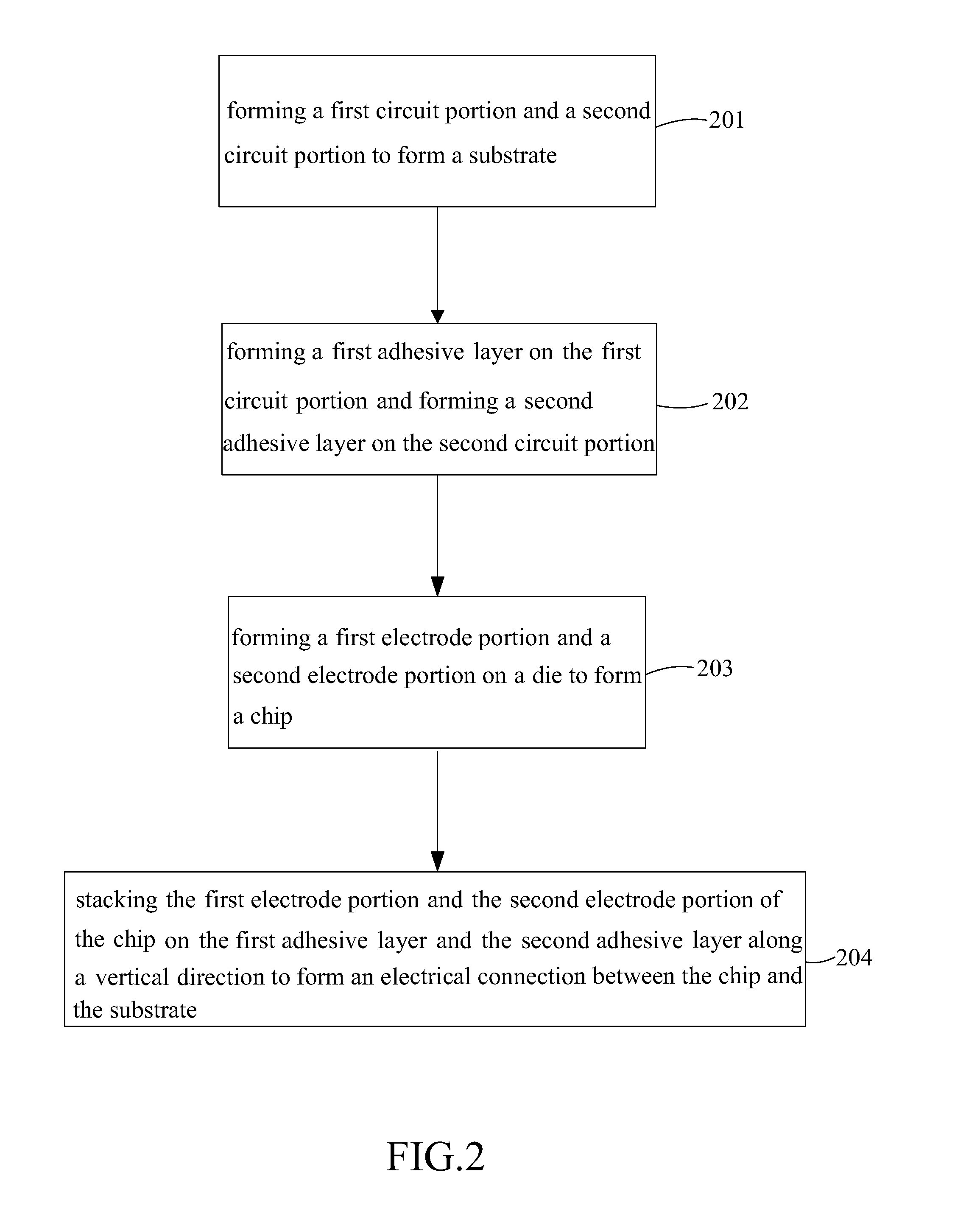
A package structure and a manufacturing method for the same are provided. The package structure includes a chip, a substrate and at least one adhesive layer. The chip has at least one electrode portion. The substrate has at least one circuit portion. The adhesive layer is disposed between the electrode portion and the circuit portion to form an electrical connection therebetween. The adhesive layer is a material, which comprises a metal compound, with a Negative Coefficient of Thermal Expansion (Negative CTE). Because of the material with a Negative CTE, the alignment shift can be avoided after the chip and the substrate are adhered together.

Description

This application claims the benefit from the priority to Taiwan Patent Application No. 100139705 filed on Nov. 1, 2011, the disclosure of which is incorporated by reference herein in its entirety.CROSS-REFERENCES TO RELATED APPLICATIONS[0001]Not applicable.BACKGROUND OF THE INVENTION[0002]1. Field of the Invention[0003]The embodiments of the present invention provide a package structure and a manufacturing method for the same. More particularly, the embodiments of the present invention provide a package structure comprising a material with a negative coefficient of thermal expansion (negative CTE) and a manufacturing method for the package structure.[0004]2. Descriptions of the Related Art[0005]As semiconductor manufacturing processes have become increasingly sophisticated and advanced over recent years, various kinds of high-performance electronic products have been developed in succession. Chips are known as the most important component in these electronic products, so the quality...

Claims


Application Information

Patent Timeline
Patent Type & Authority Applications(United States)
IPC IPC(8): H01L33/62H01L21/50
CPCH01L33/62H01L2224/16225H01L33/641
Inventor LOU, WEI-CHENGJAN, FONG-YEECHIANG, CHUNG-I
Owner WALSIN LIHWA
Why Eureka
Eureka Blog
Learn More