Ceramic electronic component and manufacturing method thereof

a technology of ceramic electronic components and manufacturing methods, applied in the direction of fixed capacitor details, stacked capacitors, fixed capacitors, etc., can solve the problems of ceramic electronic components that cannot ceramic electronic components that cannot be contaminated with water, and cracks that cannot be easily contaminated with water, and achieve high moisture resistan

Active Publication Date: 2013-05-02
MURATA MFG CO LTD
View PDF3 Cites 25 Cited by
  • Summary
  • Abstract
  • Description
  • Claims
  • Application Information

AI Technical Summary

Benefits of technology

[0025]According to various preferred embodiments of the present invention, a ceramic electronic component with high moisture resistance is provided.

Problems solved by technology

Specifically, even if electronic components undergo drop impacts, it is necessary that they will not easily become detached from mount boards and that cracks will not easily form in electronic components.
Specifically, even if mount boards undergo deflection stress caused when the mount boards are subjected to thermal expansion and contraction due to a thermal cycle, it is necessary that cracks will not easily form in ceramic electronic components and solder used for mounting.
However, there is a problem in that the ceramic electronic component disclosed in WO2004 / 053901 has low moisture resistance.

Method used


Image

  • Ceramic electronic component and manufacturing method thereof
  • Ceramic electronic component and manufacturing method thereof
  • Ceramic electronic component and manufacturing method thereof

Examples


Embodiment Construction

[0034]Preferred embodiments of the present invention will now be described. Note that the preferred embodiments described below are merely examples. The present invention is not limited to the preferred embodiments described below.

[0035]In the drawings referred to in the description of preferred embodiments, components having substantially the same function are denoted by the same reference numerals. The drawings referred in the description of preferred embodiments are schematically described, and the size ratio of objects illustrated in the drawings may be different from that of actual objects. The size ratio of objects may also be different between the drawings. The specific size ratio of objects should be judged by taking the following description into consideration.

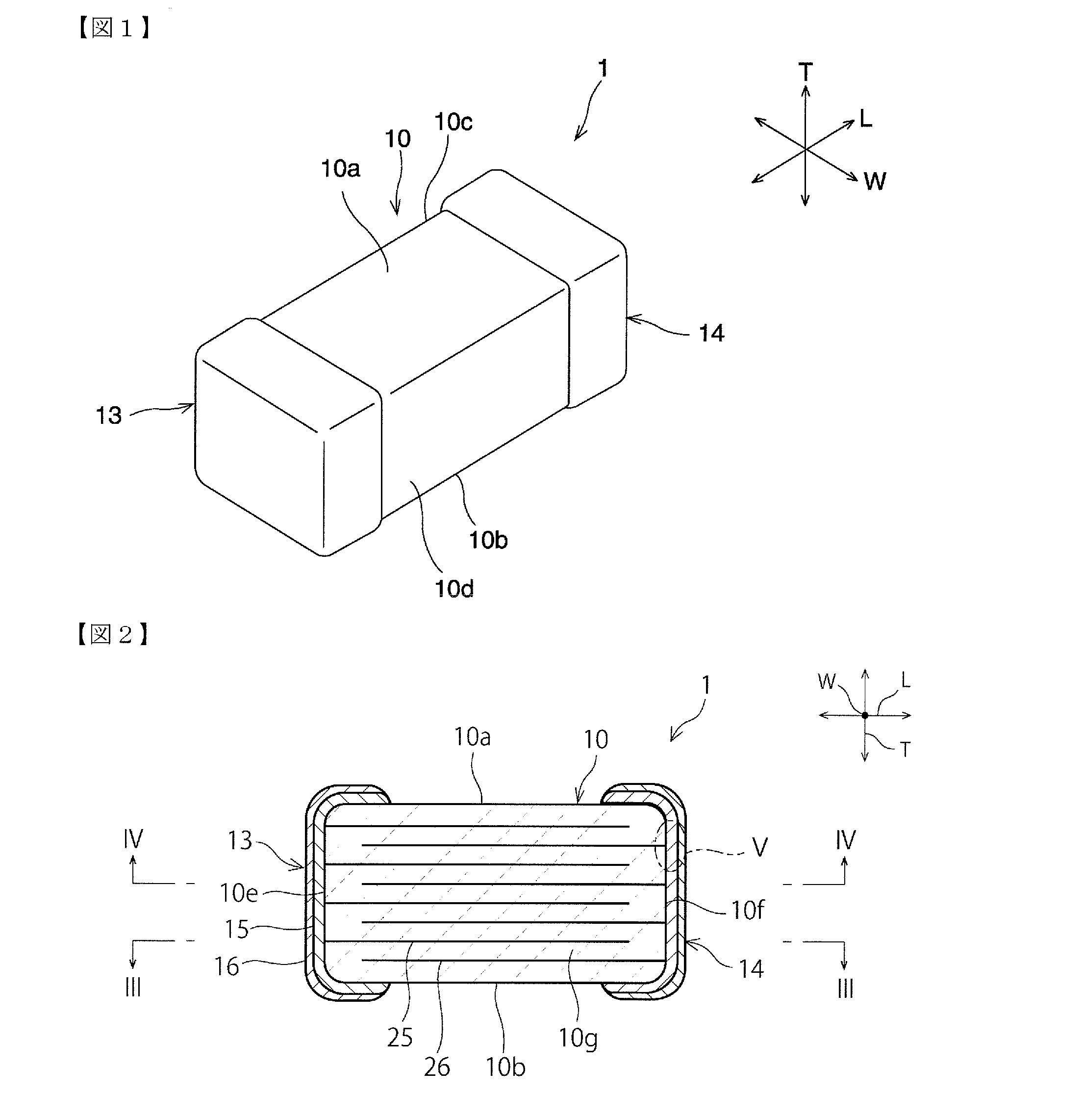
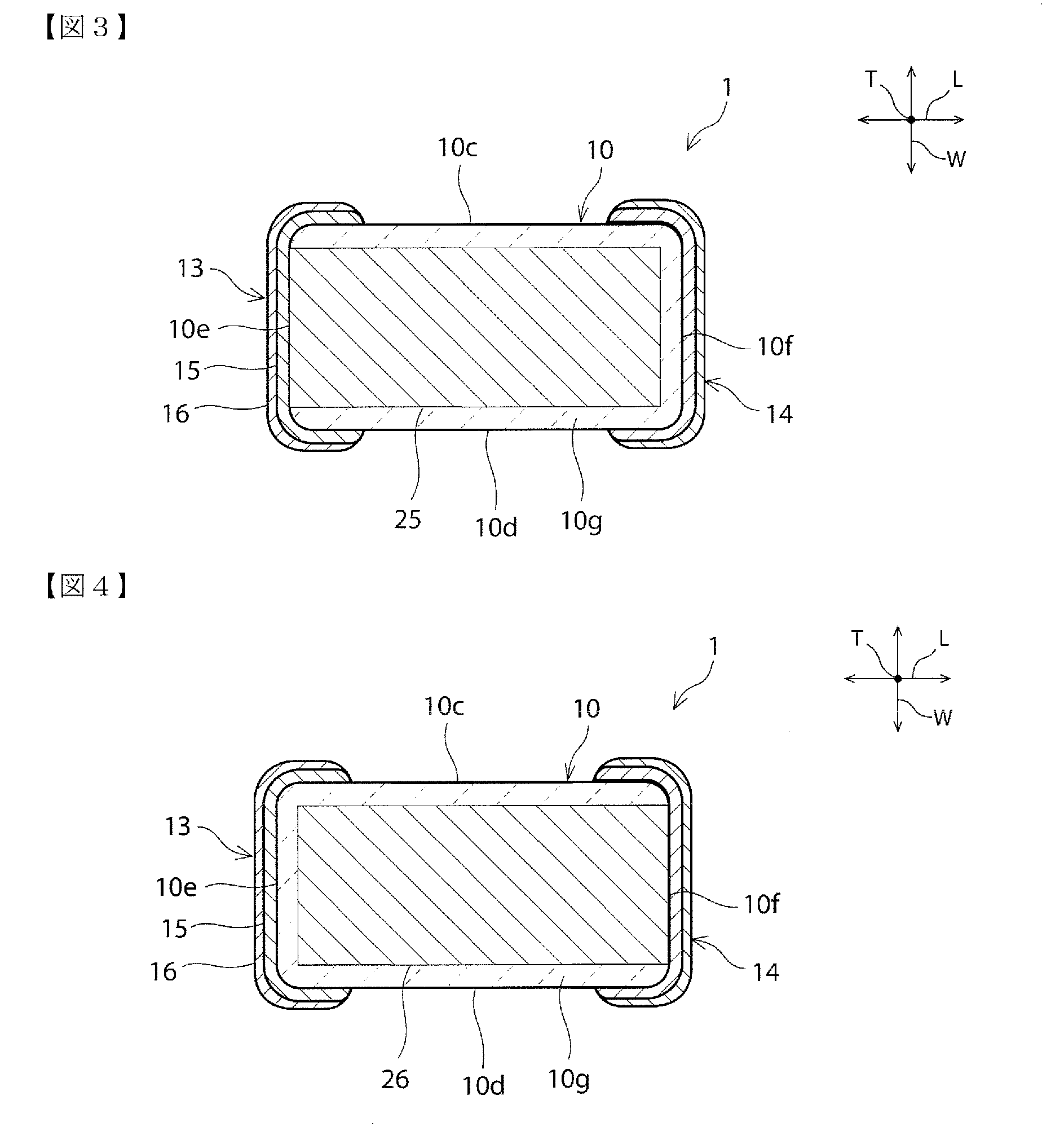
[0036]FIG. 1 is a schematic perspective view of a ceramic electronic component according to a preferred embodiment of the present invention. FIG. 2 is a schematic sectional view showing a cross section that extends in...


PUM

PropertyMeasurementUnit
temperatureaaaaaaaaaa
melting pointaaaaaaaaaa
acceleration voltageaaaaaaaaaa

Abstract

A ceramic body includes an inner electrode disposed inside the ceramic body and in which an end portion of the inner electrode extends to a surface of the ceramic body. An electrode layer is formed on the surface of the ceramic body so as to cover the end portion of the inner electrode, the electrode layer including a resin, a first metal filler that contains a first metal component, and a second metal filler that contains a second metal component having a higher melting point than the first metal component. A step of heating the electrode layer is performed to form an electrode including a metal layer that is located on the surface of the ceramic body and that includes the first and second metal components and a metal contained in the inner electrode.

Description

BACKGROUND OF THE INVENTION[0001]1. Field of the Invention[0002]The present invention relates to a ceramic electronic component and a method for producing the ceramic electronic component.[0003]2. Description of the Related Art[0004]In recent years, ceramic electronic components such as monolithic ceramic capacitors have been used in harsher environments than compared with before.[0005]Ceramic electronic components used for mobile devices such as cellular phones and portable music players are required to withstand drop impacts. Specifically, even if electronic components undergo drop impacts, it is necessary that they will not easily become detached from mount boards and that cracks will not easily form in electronic components.[0006]Electronic components used for in-vehicle equipment such as ECUs are required to withstand the shock of a thermal cycle. Specifically, even if mount boards undergo deflection stress caused when the mount boards are subjected to thermal expansion and con...

Claims


Application Information

Patent Timeline
Patent Type & Authority Applications(United States)
IPC IPC(8): H01G4/12H01G4/00
CPCH01G4/12H01G4/005H01G13/006H01G4/252H05K3/1283H05K3/4664H01G4/012H01G4/248H01G4/30
Inventor ZENZAI, KOTAOMORI, HISAYOSHIKANAYAMA, TAKASHISAKURADA, KIYOYASUSHIMIZU, NAOKIKATSUTA, SEIJIOTANI, SHINJI
Owner MURATA MFG CO LTD
Why Eureka
Try Eureka