Imprint method imprint apparatus, and article manufacturing method

a technology of imprinting apparatus and printing method, which is applied in the direction of semiconductor/solid-state device testing/measurement, semiconductor/solid-state device details, instruments, etc., can solve the problems of affecting the accuracy of superposition. , to achieve the effect of improving the superposition accuracy

Active Publication Date: 2013-05-09
CANON KK
View PDF6 Cites 26 Cited by
  • Summary
  • Abstract
  • Description
  • Claims
  • Application Information

AI Technical Summary

Benefits of technology

[0007]The present invention provides an imprint apparatus that is advantageous for improving superposition accuracy between a mold and resin on a substrate.

Problems solved by technology

However, the imprint apparatus does not have a projection optical system and the mold is brought into direct contact with the resin on the substrate, and thus, it is difficult to perform such correction.
Although the pattern section is typically formed by a drawing apparatus using an electron beam, or the like, the pattern section may also be distorted due to distortion aberration of the optical system of the drawing apparatus during formation thereof.
Furthermore, even if the pattern section can be prepared without distortion, the occurrence of distortion in a substrate-side pattern may result in an adverse effect on the superposition accuracy.
Thus, even if thermal deformation is generated on the substrate under temperature control disclosed in Japanese Patent Laid-Open No. 2004-259985, it is still difficult to sufficiently change the shape of the substrate-side pattern relative to the shape of the pattern section.

Method used


Image

  • Imprint method imprint apparatus, and article manufacturing method
  • Imprint method imprint apparatus, and article manufacturing method
  • Imprint method imprint apparatus, and article manufacturing method

Examples


first embodiment

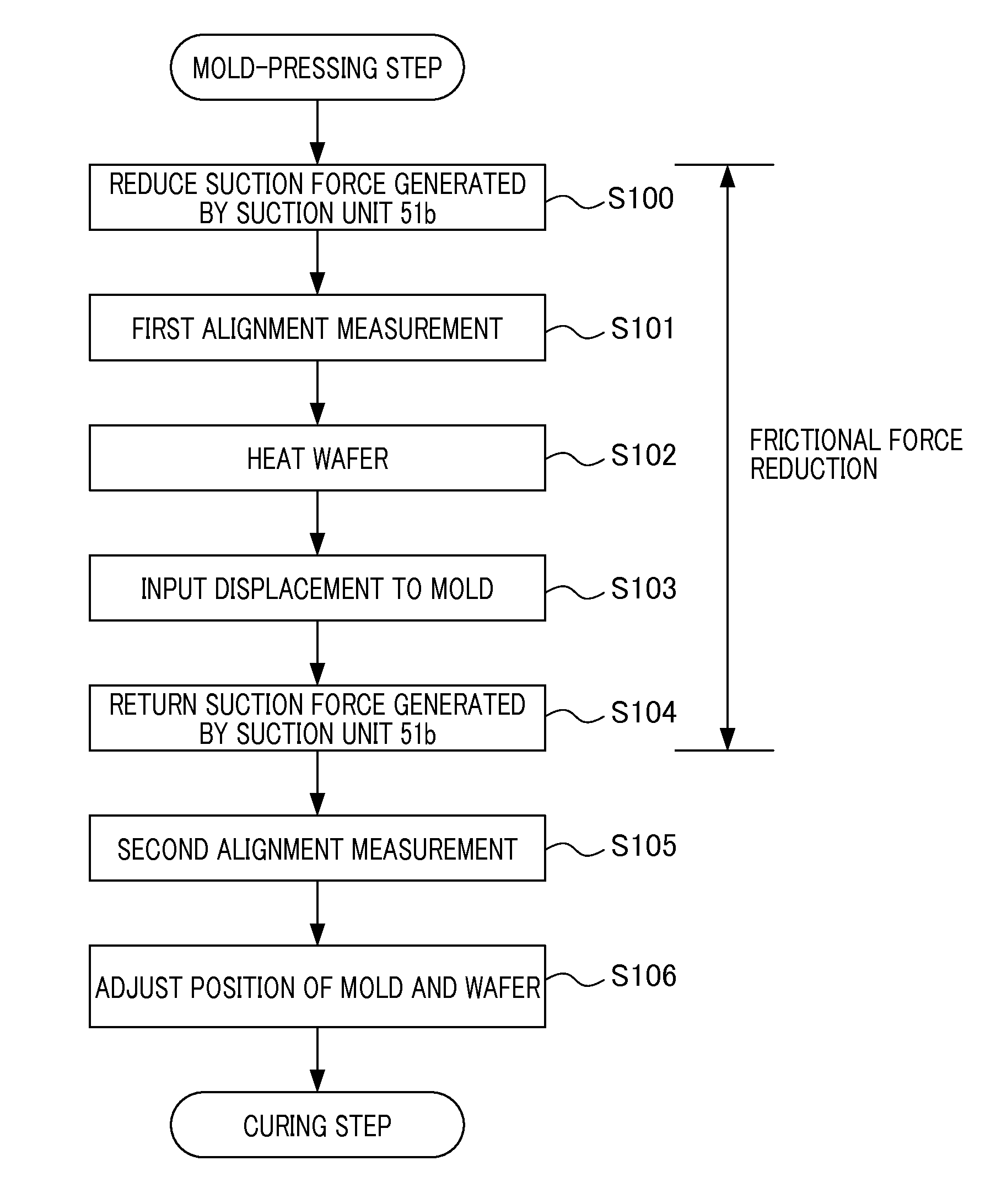
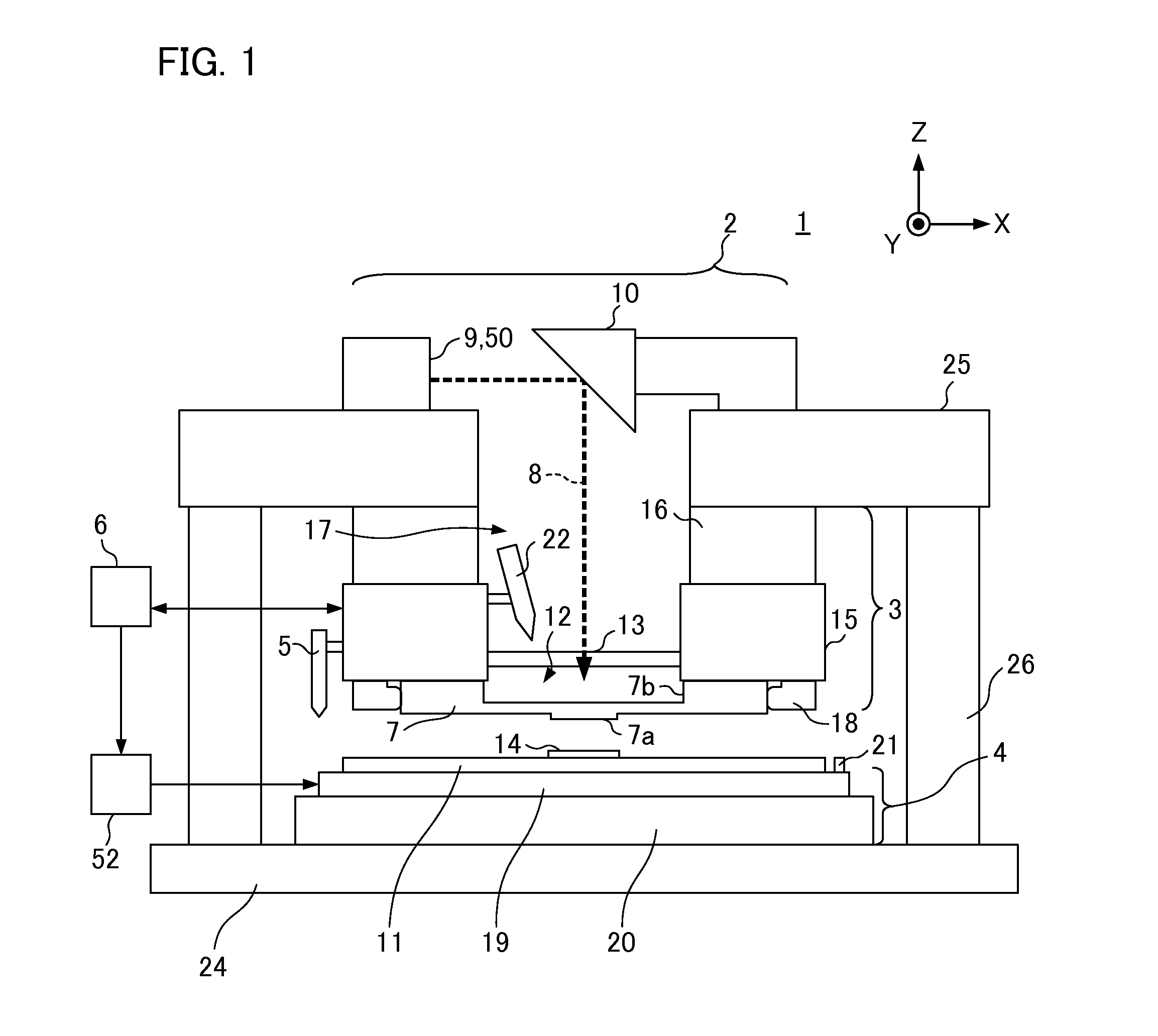
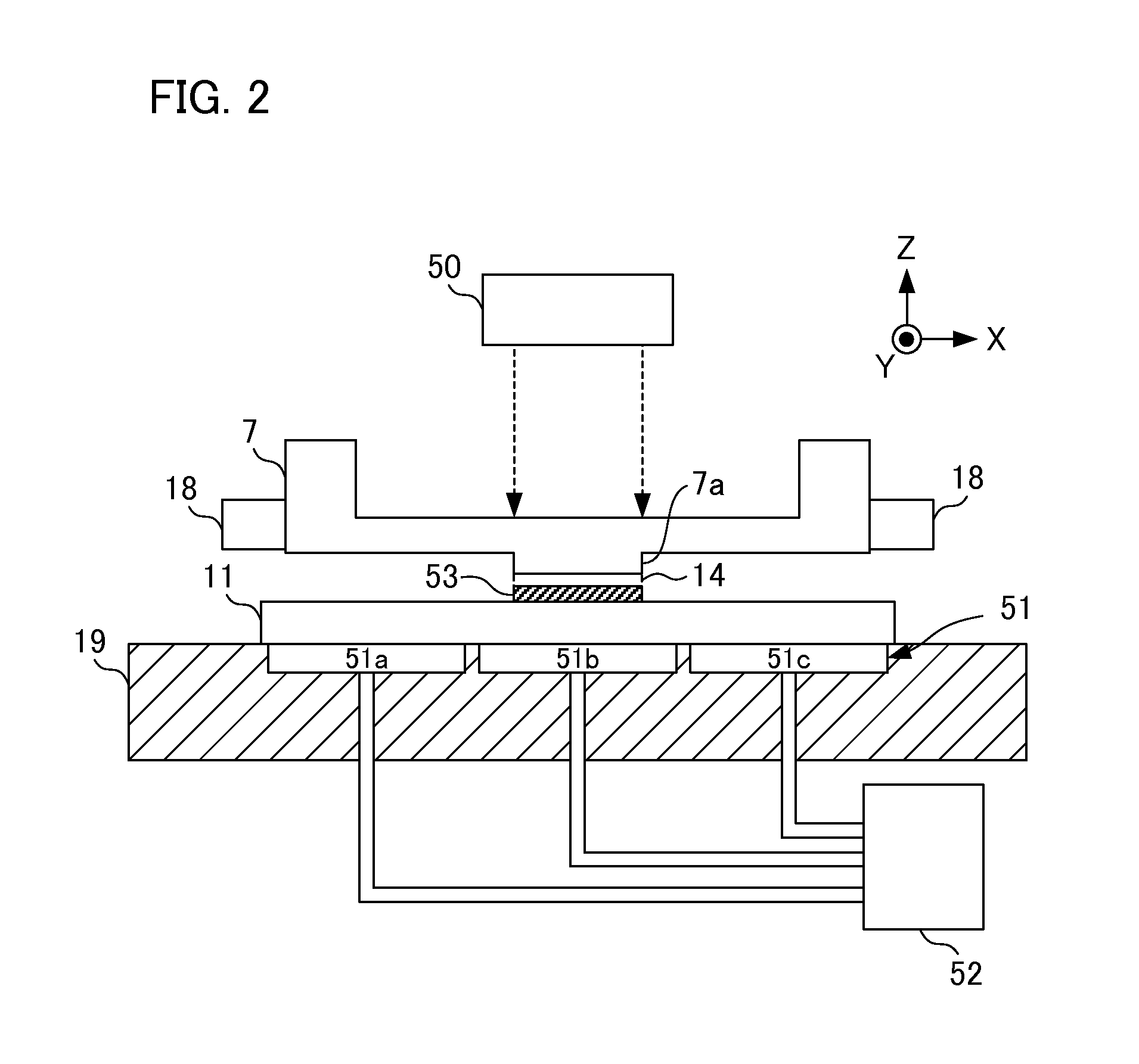
[0019]First, a description will be given of the configuration of an imprint apparatus according to a first embodiment of the present invention. FIG. 1 is a schematic diagram illustrating the configuration of an imprint apparatus 1 of the present embodiment. The imprint apparatus 1 is an apparatus that molds an uncured resin on a wafer (on a substrate), i.e., a substrate to be treated, using a mold, to thereby form a resin pattern on the wafer, which is used in the manufacture of devices, such as semiconductor devices, and the like, as articles. Note that the imprint apparatus of the present embodiment is an apparatus employing a photo-curing method. In the following drawings, a description will be given in which the Z axis is aligned parallel to the optical axis of an irradiation system that irradiates a resin on a wafer with ultraviolet light, and mutually orthogonal axes, X and Y, are aligned in a plane perpendicular to the Z axis. The imprint apparatus 1 includes a light irradiat...

second embodiment

[0036]Next, a description will be given of an imprint apparatus according to a second embodiment of the present invention. The imprint apparatus of the present embodiment has the same configuration as that of the first embodiment, but the sequence of operations from the mold-pressing step to the curing step is changed. FIGS. 4A and 4B are flowcharts illustrating the sequence of operations from the mold-pressing step to the curing step performed by the imprint apparatus 1 according to the present embodiment. First, in the example shown in FIG. 4A, after the mold-pressing step, the control unit 6 causes the magnification correction mechanism 18 to perform the displacement input to the mold 7 in step S103, in the sequence of operations of the first embodiment shown in FIG. 3, after the second alignment measurement in step S105 (step S205). Here, given that the alignment measurement in step S201 is the first alignment measurement, a step corresponding to a step S105, shown in FIG. 3, is...

third embodiment

[0038]Next, a description will be given of an input apparatus according to a third embodiment of the present invention. In the imprint apparatus of the present embodiment, the configuration of the suction units 51 provided in the wafer chuck 19 according to the first embodiment is changed. FIG. 5 is a schematic cross-sectional diagram illustrating an enlarged portion of the suction unit 51 (51a) provided in the wafer chuck 19 according to the present embodiment. The suction unit 51 has a plurality of suction pins 60 within the suction region, and a low-friction member 61 made of a low-friction material having a low friction coefficient against the wafer 11 is provided at the tip surface of each suction pin 60, i.e., the surface in contact with the rear surface of the wafer 11. Examples of such a low-friction material include DLC (diamond-like carbon). As described above, a frictional coefficient of the contact surface between the wafer chuck 19 and the wafer 11 is reduced, and thus,...


PUM

PropertyMeasurementUnit
shapeaaaaaaaaaa
static frictional forceaaaaaaaaaa
frictional forceaaaaaaaaaa

Abstract

An imprint method of transferring a pattern formed on a mold onto a resin on a substrate. The substrate is held on a holding surface in a holding step. A shape of a substrate-side pattern area where the pattern is formed on the substrate is deformed in a deforming step. A resin on the deformed substrate-side pattern area is brought into contact with the mold in a contacting step. The resin is cured in a curing step, and the mold is released from the resin in contact with the mold in a mold-releasing step. In the deforming step, a deformation force, which is greater than a maximum static frictional force acting between a rear surface of the substrate corresponding to the substrate-side pattern area and the holding surface, is applied to the substrate in a direction along the surface thereof.

Description

BACKGROUND OF THE INVENTION[0001]This application claims the benefit of Japanese Patent Application No. 2011-226636, filed Oct. 14, 2011, and Japanese Patent Application No. 2012-220209, filed Oct. 2, 2012, which are hereby incorporated by reference herein in their entirety.FIELD OF THE INVENTION[0002]The present invention relates to an imprint method, an imprint apparatus, and an article manufacturing method.DESCRIPTION OF THE RELATED ART[0003]As the demand for microfabrication of semiconductor devices or MEMS increases, not only has conventional photolithography technology, but also, microfabrication technology, in which an uncured resin on a substrate is molded by a mold to thereby form a resin pattern on the substrate, has been receiving attention. This technology is also referred to as “imprint technology”, by which a fine structure with dimensions of a few nanometers can be formed on a substrate. One example of the imprint technology includes a photo-curing method. An imprint ...

Claims


Application Information

Patent Timeline
Patent Type & Authority Applications(United States)
IPC IPC(8): G03F7/00
CPCG03F7/0002B82Y40/00B82Y10/00B29C59/026H01L21/0273B29C59/16B29K2101/00B29L2009/00B29L2031/34B29C35/0805B29C2035/0822H01L21/0271H01L21/324H01L21/67115H01L21/6715H01L21/682H01L21/6838H01L22/20H01L23/544
Inventor NAKAGAWA, KAZUKIHASEGAWA, NORIYASUMURAKAMI, YOSUKEMATSUMOTO, TAKAHIRO
Owner CANON KK
Why Eureka
Try Eureka