NAND flash with non-trapping switch transistors

a switch transistor and non-trapping technology, applied in the field of flash memory technology, can solve the problems of limiting the ability to increase the density of flash memory, affecting device performance, and affecting so as to reduce or eliminate the ability of the structure to trap charg

Active Publication Date: 2013-05-16
MACRONIX INT CO LTD
View PDF5 Cites 50 Cited by
  • Summary
  • Abstract
  • Description
  • Claims
  • Application Information

AI Technical Summary

Benefits of technology

[0009]A memory device is described that can comprise a three-dimensional 3D array of memory cells including dielectric charge trapping structures, having a plurality of switch transistors including gate dielectrics different than the dielectric charge trapping structures. The gate dielectrics include modified dielectric charge trapping structures in some examples, where the modifications reduce or eliminate the ability of the structure to trap charge.

Problems solved by technology

As the density increases in memory devices, and the floating gate memory cells get closer and closer together, interference between the charge stored in adjacent floating gates becomes a problem.
This is limiting the ability to increase the density of flash memory based on floating gate memory cells.
This can impact device performance in a number of undesirable ways.

Method used


Image

  • NAND flash with non-trapping switch transistors
  • NAND flash with non-trapping switch transistors
  • NAND flash with non-trapping switch transistors

Examples


Embodiment Construction

[0034]A detailed description of embodiments of the present invention is provided with reference to the FIGS. 1-24.

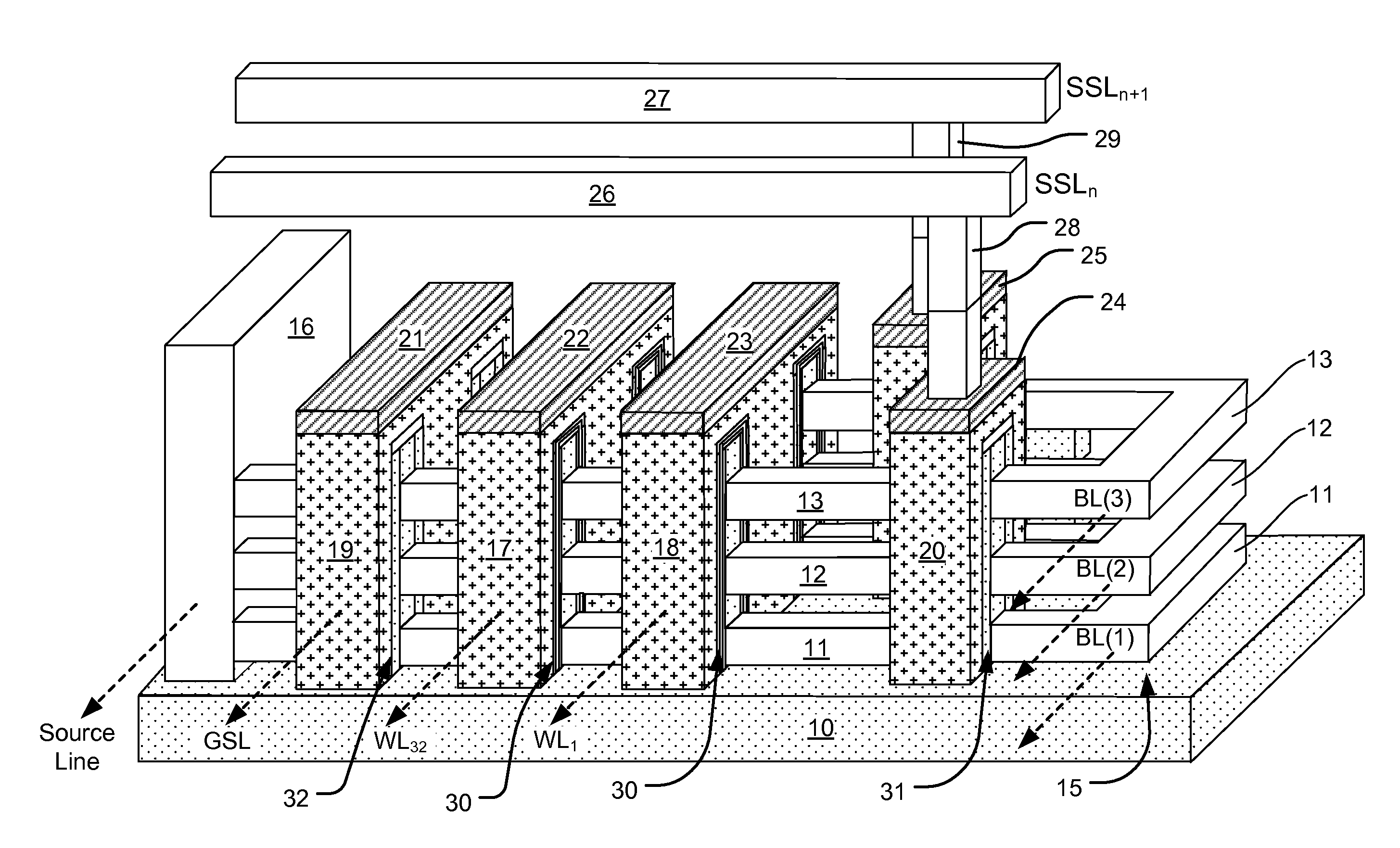
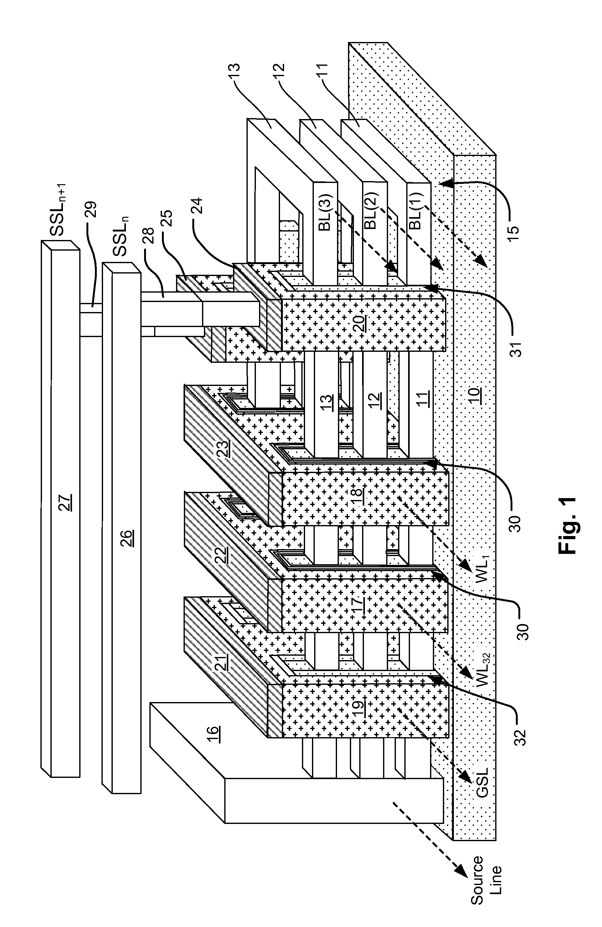
[0035]FIG. 1 is a simplified view of a 3D memory having dielectric fill removed to reveal structures of the 3D memory, based on the memory described in our publication, Lue et al., “A Highly Scalable 8-Layer 3D Vertical-Gate (VG) TFT NAND Flash Using Junction-Free Buried Channel BE-SONOS Device,” 2010 Symposium on VLSI Technology Digest of Technical Papers, pages 131-132 (Symposium held in June 2010). The structure shown in FIG. 1 comprises a 3D array of memory cells which have dielectric charge trapping structures 30 in a NAND architecture including stacks of NAND strings of memory cells. The structure includes a plurality of switch transistors coupled to the NAND string. The switch transistors include gate dielectrics 31 and 32 that are different than the dielectric charge trapping structures 30 in the memory cells.

[0036]The 3D array includes a plurality of the stacks ...


PUM


Abstract

A manufacturing method for a memory array includes first forming a multilayer stack of dielectric material on a plurality of semiconductor strips, and then exposing the multilayer stack in switch transistor regions. The multilayer stacks exposed in the switch transistor regions are processed to form gate dielectric structures that are different than the dielectric charge trapping structures. Word lines and select lines are then formed. A 3D array of dielectric charge trapping memory cells includes stacks of NAND strings of memory cells. A plurality of switch transistors are coupled to the NAND strings, the switch transistors including gate dielectric structures wherein the gate dielectric structures are different than the dielectric charge trapping structures.

Description

BACKGROUND[0001]1. Field[0002]The present invention relates to flash memory technology.[0003]2. Description of Related Art[0004]Flash memory is a class of non-volatile integrated circuit memory technology. Traditional flash memory employs floating gate memory cells. As the density increases in memory devices, and the floating gate memory cells get closer and closer together, interference between the charge stored in adjacent floating gates becomes a problem. This is limiting the ability to increase the density of flash memory based on floating gate memory cells. Another type of memory cell used for flash memory can be referred to as a charge trapping memory cell, which uses a dielectric charge trapping structure in place of the floating gate. Charge trapping memory cells use dielectric material for charge storage that does not cause cell-to-cell interference like that encountered with floating gate technology.[0005]The typical charge trapping flash memory cell consists of a field ef...

Claims


Application Information

Patent Timeline
Patent Type & Authority Applications(United States)
IPC IPC(8): H01L29/792H01L21/336
CPCH01L27/11578H01L27/1157H10B43/20H10B43/35
Inventor CHEN, SHIH-HUNGLUE, HANG-TINGSHIH, YEN-HAO
Owner MACRONIX INT CO LTD
Why Eureka
Try Eureka