
High frequency resistor

a high frequency resistor and resistor technology, applied in the direction of resistor details, resistor mounting/supporting, coatings, etc., can solve the problems of not disclosing any frequency compensation, negatively affecting the high frequency response of the resistor, and alumina substrates, etc., to achieve the effect of improving the resistor

Active Publication Date: 2013-05-23
KYOCERA AVX COMPONENTS CORP
View PDF5 Cites 3 Cited by
  • Summary
  • Abstract
  • Description
  • Claims
  • Application Information

AI Technical Summary

Benefits of technology

The present patent is about a new type of resistor that solves certain problems in the field of resistor technology. The new resistor has a frequency compensating conductive layer that is positioned over a resistive layer with contact pads. This conductive layer can be made of aluminum or other materials and can be in contact with or not in contact with the contact pads. The new resistor also has a layer of adhesive material between the substrate and the resistive layer, which forms a sandwich structure. The new resistor can be used in surface mount technology and has improved performance.

Problems solved by technology

According to Lai et al., it had been recognized that untrimmed edges of thin film resistive layers had negatively impacted resistor high frequency response.
The device provides an alumina substrate and does not disclose any form of frequency compensation.

Method used


Image

  • High frequency resistor
  • High frequency resistor
  • High frequency resistor

Examples


Embodiment Construction

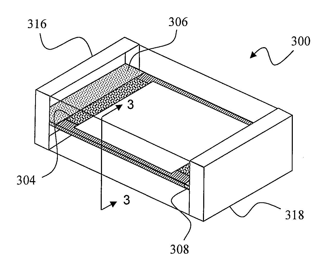
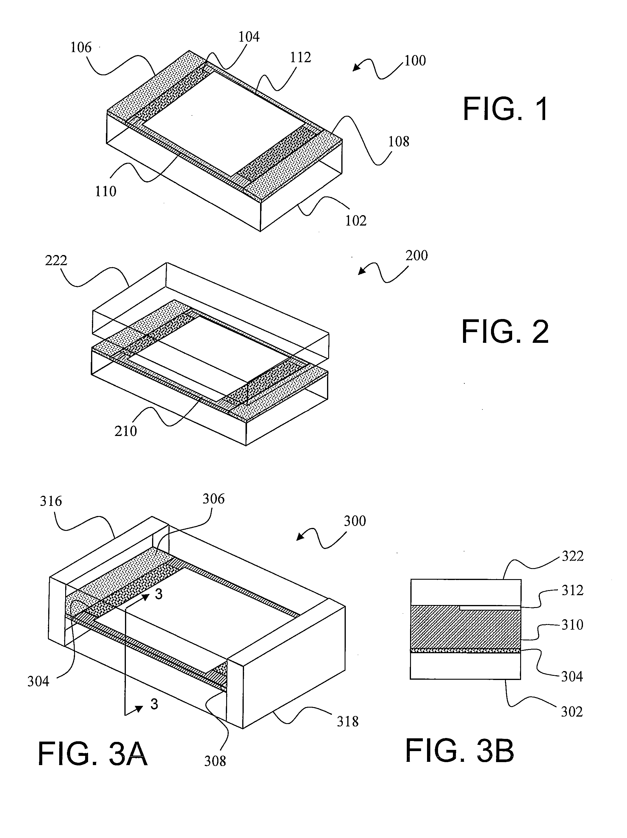
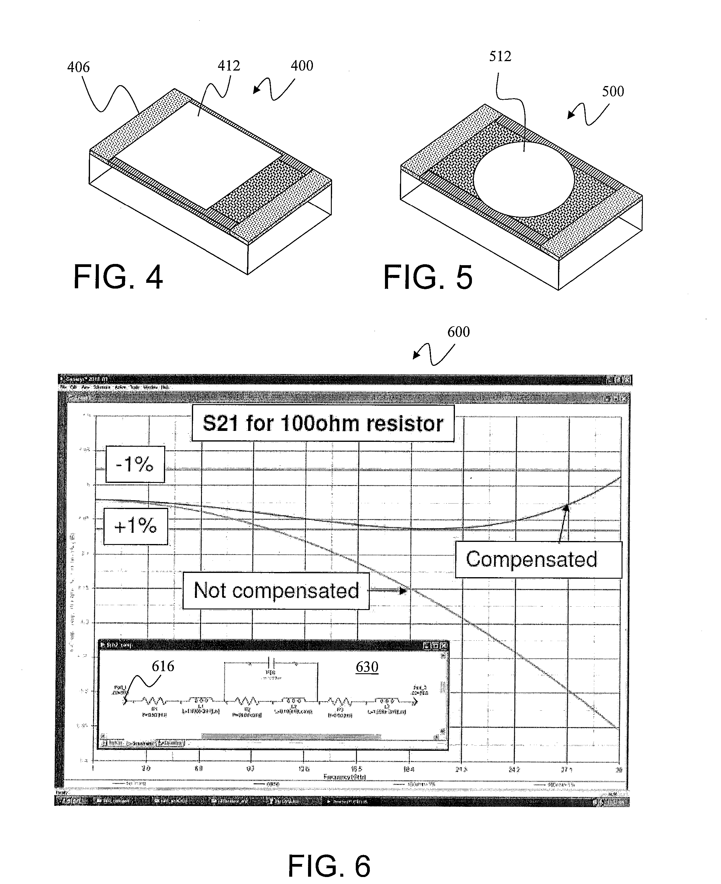
[0045]As referenced in the Brief Summary of the Subject Matter section, aspects of the presently disclosed subject matter are directed towards an improved frequency compensated surface mount thin film resistor. Referring to the drawings, FIG. 1 illustrates an exemplary partially completed ultra wideband resistor generally 100 in accordance with presently disclosed technology. Ultra wideband resistor 100 corresponds to a layer of resistive material 104 formed on substrate 102 and extending at least to and in contact with conductive contact pads 106, 108 formed at opposite ends of substrate 102. In accordance with various specific embodiments of the presently disclosed subject matter, substrate 102 may correspond to a glass substrate, resistive material 104 may correspond to a layer of tantalum nitride (TaN), and conductive contact pads 106, 108 may correspond to layers of copper (Cu). Those of ordinary skill in the art will appreciate, however, that other materials may be used for an...


PUM

PropertyMeasurementUnit
Timeaaaaaaaaaa
Thicknessaaaaaaaaaa
Flexibilityaaaaaaaaaa

Abstract

An ultra wideband frequency compensated resistor and related methodologies for frequency compensation are disclosed. In exemplary configuration, a resistive layer is provided over a substrate, and a frequency compensating structure is provided over at least a portion of the resistive layer and separated therefrom by an insulative layer. In certain embodiments, the insulating layer may be an adhesive that may also be effective to secure a protective cover over the resistive material and supporting substrate. In selected embodiments, the frequency compensating structure corresponds to a plurality of conductive layers, one or more of which may be directly electrically connected to terminations for the resistive material while one or more of the conductive layers are not so connected.

Description

PRIORITY CLAIM[0001]This application claims the benefit of previously filed U.S. Provisional Patent Application entitled “HIGH FREQUENCY RESISTOR,” assigned U.S. Ser. No. 61 / 561,334, filed Nov. 18, 2011, and which is incorporated herein by reference for all purposes.FIELD OF THE SUBJECT MATTER[0002]The presently disclosed subject matter relates generally to electrical resistors and particularly to ultra wide band surface mount resistors employing thin film technology.BACKGROUND OF THE SUBJECT MATTER[0003]Surface mounting has become the preferred technique for circuit board assembly such that numerous if not nearly all types of electronic components have been or are being redesigned for surface mount (that is, leadless) applications. The rapid incorporation of surface mount devices (SMD) into all types of electronic circuits has created a demand for high frequency resistors.[0004]Resistors serve an essential function on many circuit boards. There are many different performance charac...

Claims


Application Information

Patent Timeline
IPC IPC(8): H01C7/00H01C17/00
CPCH01C7/003Y10T29/49117H01C1/01H01C17/06513H01C1/142H01C1/06
Inventor KORONY, GHEORGHECHRISTIAN, KEVIN D.
Owner KYOCERA AVX COMPONENTS CORP
Learn More