Multi-layered printed circuit board and manufacturing method thereof

a printed circuit board and multi-layer technology, applied in the direction of printed circuit parts, printed element electric connection formation, cable/conductor manufacturing, etc., can solve the problem of possible jeopardization of reliability

Inactive Publication Date: 2013-06-13
SAMSUNG ELECTRO MECHANICS CO LTD
View PDF4 Cites 3 Cited by
  • Summary
  • Abstract
  • Description
  • Claims
  • Application Information

AI Technical Summary

Benefits of technology

[0008]Embodiments of the present invention provide a multi-layered printed circuit board and a ma

Problems solved by technology

In the meantime, in case the inner-layer circuit wiring is formed to be thick, void may be occurred in an interface between a

Method used


Image

  • Multi-layered printed circuit board and manufacturing method thereof
  • Multi-layered printed circuit board and manufacturing method thereof
  • Multi-layered printed circuit board and manufacturing method thereof

Examples


Embodiment Construction

[0022]Since there can be a variety of permutations and embodiments of the present invention, certain embodiments will be illustrated and described with reference to the accompanying drawings. This, however, is by no means to restrict the present invention to certain embodiments, and shall be construed as including all permutations, equivalents and substitutes covered by the ideas and scope of the present invention. Throughout the description of the present invention, when describing a certain technology is determined to evade the point of the present invention, the pertinent detailed description will be omitted.

[0023]Hereinafter, a multi-layered printed circuit board in accordance with an embodiment of the present invention will be described with reference to the accompanying drawings.

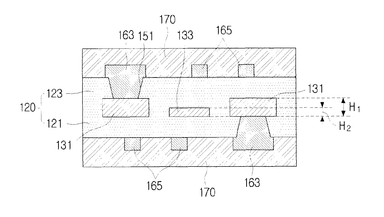
[0024]FIG. 1 shows a multi-layered printed circuit board in accordance with an embodiment of the present invention.

[0025]Referring to FIG. 1, the multi-layered printed circuit board can include an insu...


PUM


Abstract

A multi-layered printed circuit board and a method of manufacturing the multi-layered printed circuit board are disclosed. The multi-layered printed circuit board in accordance with an embodiment of the present invention includes: an insulation layer; an inner-layer pad disposed inside the insulation layer; an inner-layer circuit wiring disposed inside the insulation layer and formed to be thinner than that of the inner-layer pad; a via connected with the inner-layer pad by penetrating the insulation layer; and an outer-layer circuit wiring formed on an outside surface of the insulation layer.

Description

CROSS-REFERENCE TO RELATED APPLICATIONS[0001]This application claims the benefit of Korean Patent Application No. 10-2011-0131972, filed with the Korean Intellectual Property Office on Dec. 9, 2011, the disclosure of which is incorporated herein by reference in its entirety.BACKGROUND[0002]1. Technical Field[0003]The present invention relates to a multi-layered printed circuit board that can be manufactured in a thin type and a method of manufacturing the multi-layered printed circuit board.[0004]2. Background Art[0005]An increasing number of electronic parts are mounted in electronic devices because printed circuit boards have increasingly become thinner, more integrated, minuter and more functional.[0006]To make a printed circuit board thinner, the insulating material and the inner-layer circuit wiring need to be made thinner. As the inner-layer circuit wiring and the inner-layer pad of a multi-layered printed circuit board are formed by etching a metal layer, the inner-layer circ...

Claims


Application Information

Patent Timeline
IPC IPC(8): H05K3/06H05K1/02
CPCH05K3/06H05K1/0298H05K1/0203H05K1/116H05K2203/1476H05K3/4682H05K2201/09736H05K2203/0369H05K3/4652H05K3/46H05K3/40
Inventor CHIO, JONG-GYUSHIN, GIL-YONGYOON, KYOUNG-RO
Owner SAMSUNG ELECTRO MECHANICS CO LTD
Why Eureka
Try Eureka