Slew rate modulation

Active Publication Date: 2013-06-13
MICRON TECH INC
View PDF6 Cites 16 Cited by
  • Summary
  • Abstract
  • Description
  • Claims
  • Application Information

AI Technical Summary

Problems solved by technology

This slew rate can be inconsistent, however, if there is a skewed edge in the control signal.
The inconsistent sl

Method used


Image

  • Slew rate modulation
  • Slew rate modulation
  • Slew rate modulation

Examples


Embodiment Construction

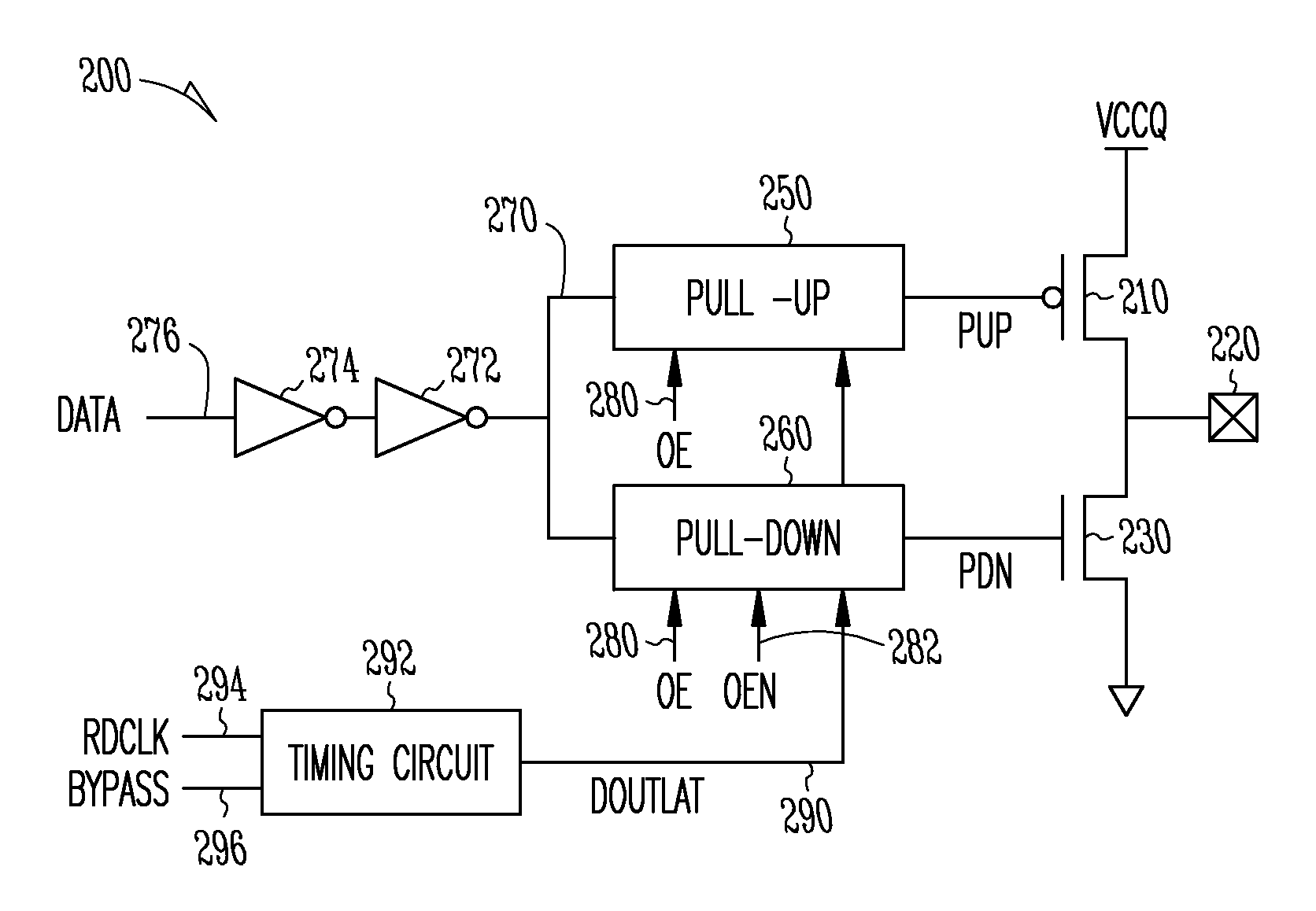
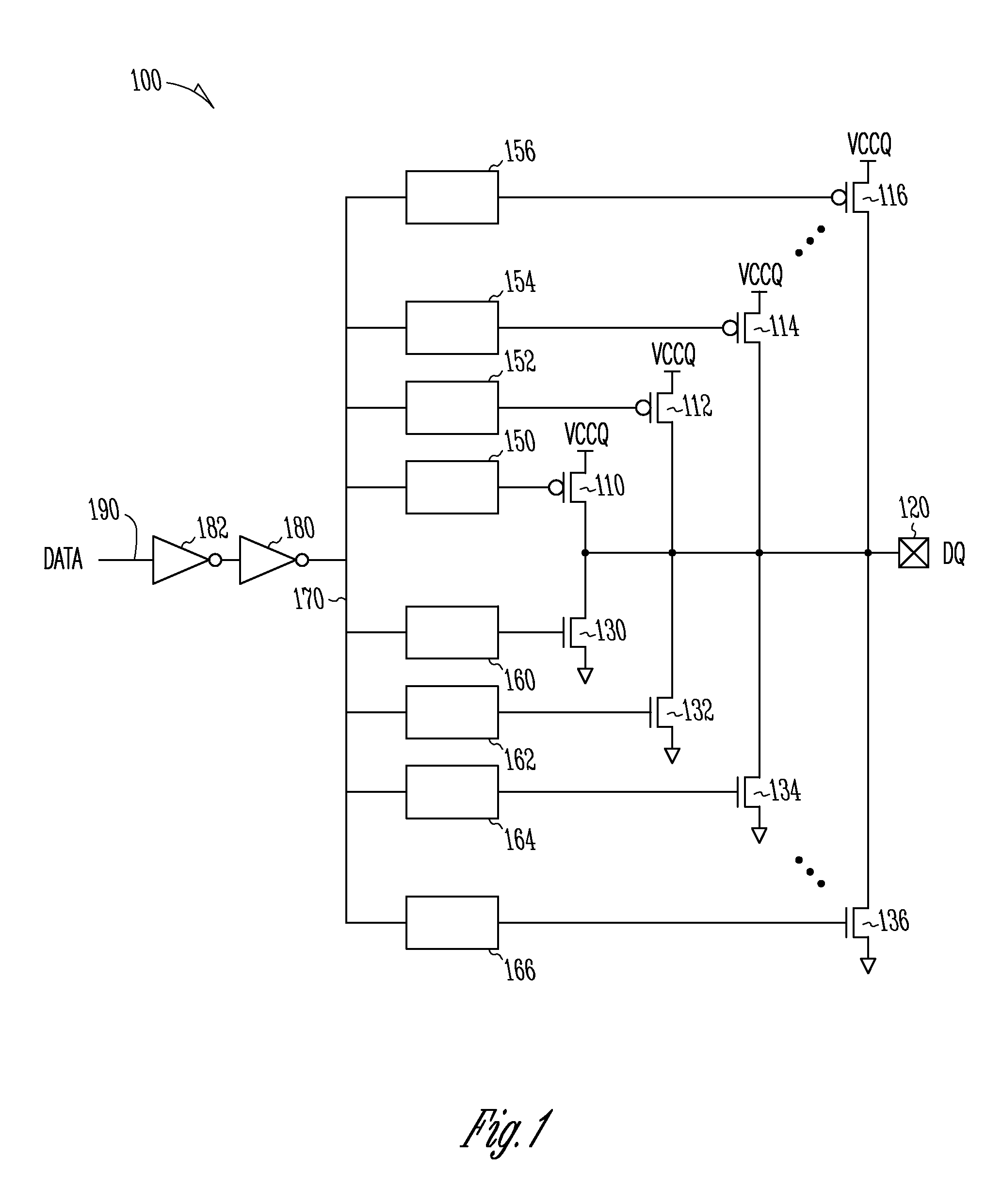
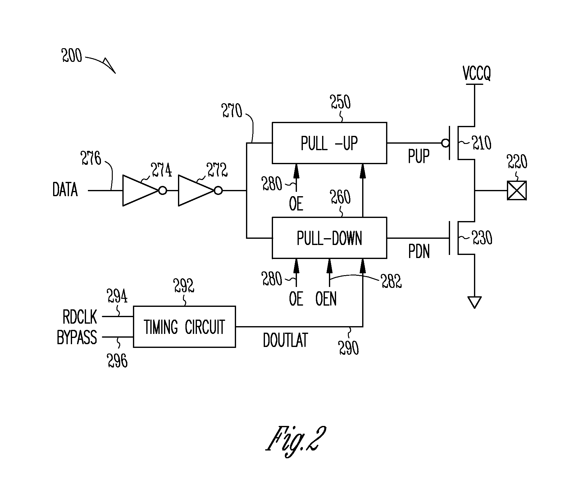
[0016]An array of charge storage devices according to various embodiments of the invention may function as an array of memory cells in a memory device such as a NOT AND (NAND) memory device.

[0017]In this description, a transistor is described as being switched on to assume an activated state when it is rendered conductive by a control gate voltage that is separated from its source voltage by at least its threshold voltage. The transistor is described as being switched off to assume an inactive state when the difference between the control gate voltage and the source voltage is less than the threshold voltage, so that the transistor is rendered non-conductive.

[0018]A slew rate is the rate of change of voltage (voltage change / time) that a driver circuit can provide (e.g., generate) at a data (DQ) node when the driver circuit is changing a signal it is driving on the DQ node. The driver circuit may change the signal from logic low to logic high or logic high to logic low. The slew rate...


PUM


Abstract

Apparatus and methods may operate so that arrival times of a data signal at gates of transistors are controlled to switch the transistors at different times to modulate the slew rate of a signal on a node. Additional embodiments are also described.

Description

BACKGROUND[0001]Non-volatile semiconductor memories (NVSMs) are widely used in electronic devices such as personal digital assistants (PDAs), laptop computers, mobile phones and digital cameras. A NVSM can transmit data to a bus at substantial rates.BRIEF DESCRIPTION OF THE DRAWINGS[0002]Some embodiments are illustrated by way of example and not limitation in the figures of the accompanying drawings in which:[0003]FIG. 1 is an electrical schematic diagram of an apparatus in the form of a driver circuit according to various embodiments of the invention;[0004]FIG. 2 is an electrical schematic diagram of an apparatus in the form of a driver circuit according to various embodiments of the invention;[0005]FIG. 3 is an electrical schematic diagram of an apparatus in the form of a pull-up circuit according to various embodiments of the invention;[0006]FIG. 4 is an electrical schematic diagram of an apparatus in the form of a pull-down circuit according to various embodiments of the inventi...

Claims


Application Information

Patent Timeline
IPC IPC(8): H03K5/12
CPCH03K19/0027H03K19/018585H03K19/018528G11C7/12G11C16/24
Inventor SONG, DAESIK
Owner MICRON TECH INC
Why Eureka
Try Eureka