Stacked RRAM Array With Integrated Transistor Selector

a transistor selector and array technology, applied in semiconductor devices, digital storage, instruments, etc., can solve the problems of large parasitic current flowing through non-selectable memory cells, raw cross-point arrays suffering from read errors, sneak currents, etc., and achieve the effect of reducing sneak currents

Active Publication Date: 2013-06-27
INTERUNIVERSITAIR MICRO ELECTRONICS CENT (IMEC VZW)
View PDF13 Cites 20 Cited by
  • Summary
  • Abstract
  • Description
  • Claims
  • Application Information

AI Technical Summary

Benefits of technology

[0035]It is an advantage of embodiments of the present invention that cells with the smallest cell size in a raw cross-point array can be realized, thereby, however, reducing sneak currents compared to a prior art raw cross-point array, or even avoiding these.

Problems solved by technology

Such raw cross-point arrays with single RRAM elements lead to a large parasitic current flowing through non-selected memory cells.
Hence raw cross-point arrays suffer from READ errors (sneak currents) and possibly from PROGRAM errors, as well as from excessive current and power consumption.
Disadvantages of solutions including a selector 5 in each cell are the increase of the cell size, hence the reduced memory density, the more complex processing—not a simple cross-point array but requiring the definition of intermediate pillar elements—the fact that no appropriate two-terminal bipolar selector devices have been identified.

Method used


Image

  • Stacked RRAM Array With Integrated Transistor Selector
  • Stacked RRAM Array With Integrated Transistor Selector
  • Stacked RRAM Array With Integrated Transistor Selector

Examples


Embodiment Construction

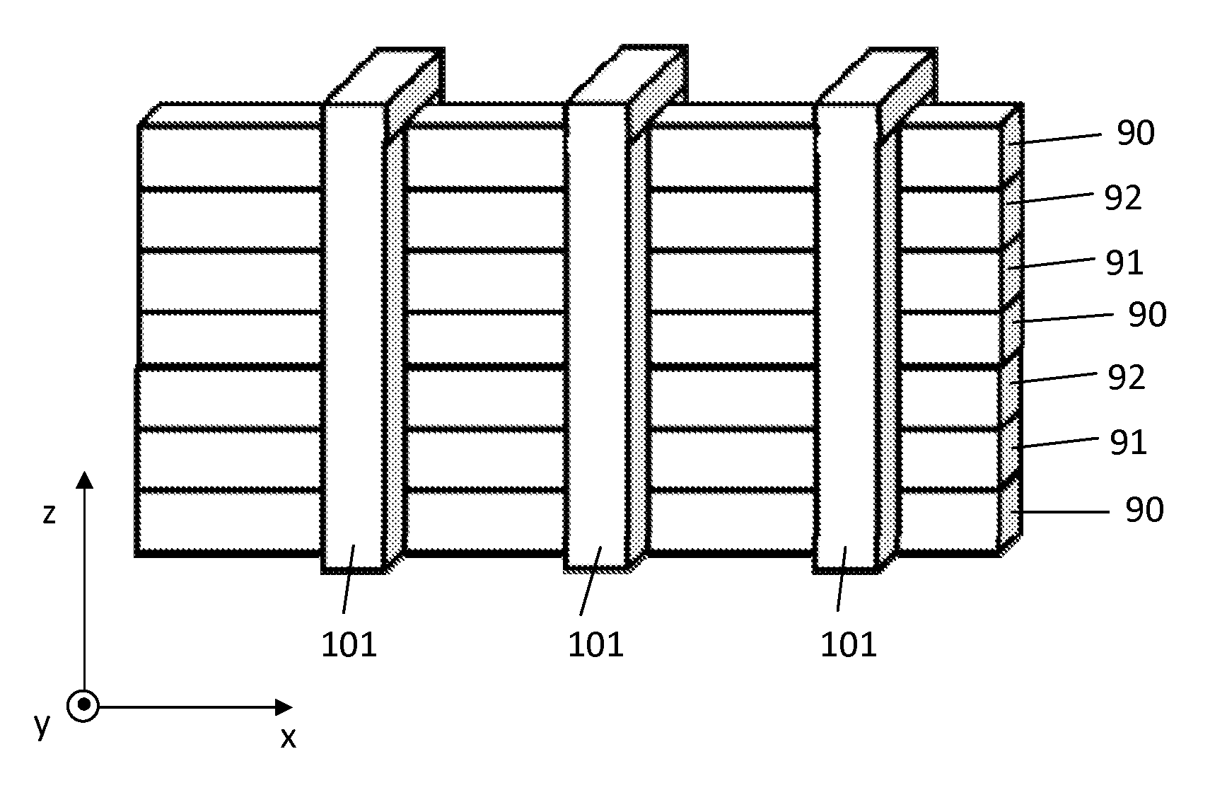
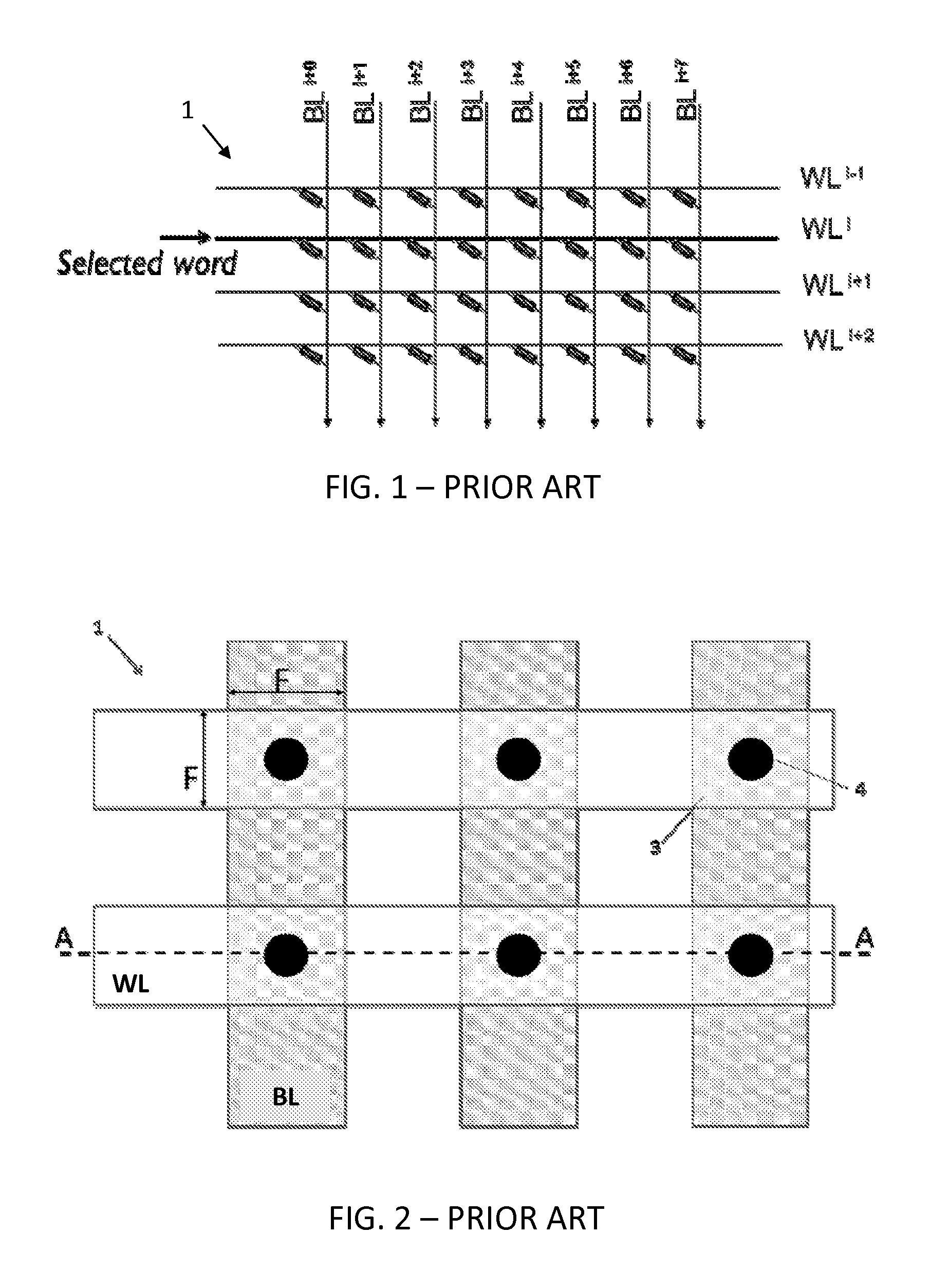
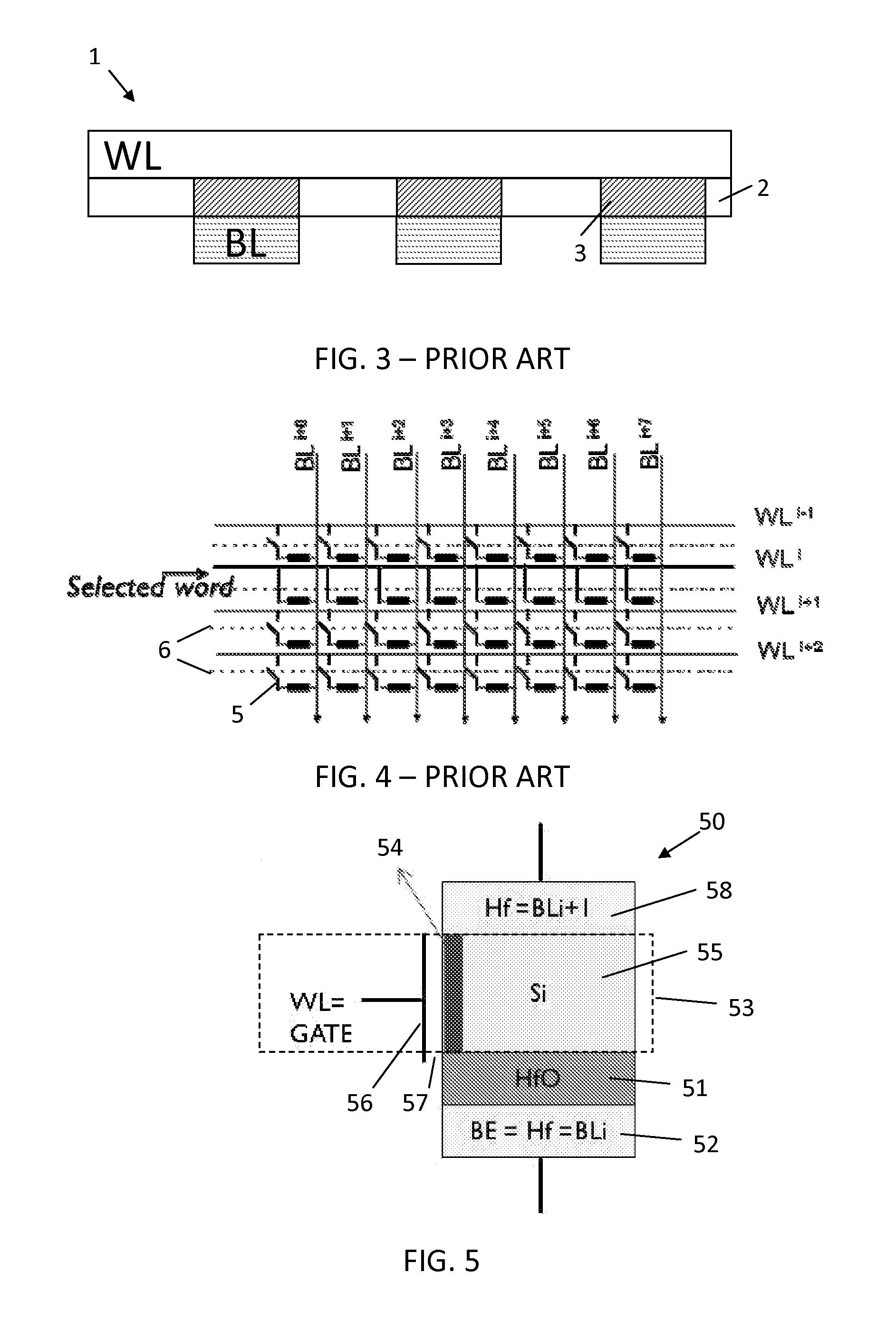
[0055]The present invention will be described with respect to particular embodiments and with reference to certain drawings but the invention is not limited thereto but only by the claims.

[0056]The terms first, second, and the like in the description and in the claims are used for distinguishing between similar elements and not necessarily for describing a sequence, either temporally, spatially, in ranking or in any other manner. It is to be understood that the terms so used are interchangeable under appropriate circumstances and that the embodiments of the invention described herein are capable of operation in other sequences than described or illustrated herein.

[0057]Moreover, the terms top, under, and the like in the description and the claims are used for descriptive purposes and not necessarily for describing relative positions. It is to be understood that the terms so used are interchangeable under appropriate circumstances and that the embodiments of the invention described h...


PUM


Abstract

The present invention provides a resistive memory array arranged in a 3D stack comprising a plurality of resistivity switching memory elements laid out in an array in a first and second direction, and stacked in a third direction, a plurality of first electrodes and a plurality of second electrodes extending in the first direction, each first electrode and each second electrode being associated with the at least one resistivity switching memory element, and a plurality of transistor devices, each transistor device being electrically coupled to one of the resistivity switching memory elements, an inversion or accumulation channel of a transistor device being adapted for forming a switchable resistivity path in the third direction, between the electrically coupled resistivity switching memory element and the associated second electrode, wherein the memory array furthermore comprises at least one third electrode provided in a trench through the stack.

Description

CROSS-REFERENCE TO RELATED APPLICATION[0001]This application claims priority to European Patent Application No. 11195473.1 filed on Dec. 23, 2011, the contents of which are hereby incorporated by reference.FIELD OF THE INVENTION[0002]The present invention relates to semiconductor memory devices, more particularly for example to arrays of non-volatile memory cells comprising a reversible resistance switching layer, their resistance value being representative of the data stored in the memory cell. The present invention in particular relates to a new array design for minimizing design area and to methods of fabrication thereof.BACKGROUND OF THE INVENTION[0003]A resistive memory device, such as for example the electrically programmable resistive cross point memory device as described in US2003 / 0003674, is a non-volatile memory device which generally comprises an active layer capable of having its resistivity changed in response to an electrical signal, interposed between a plurality of ...

Claims


Application Information

Patent Timeline
Patent Type & Authority Applications(United States)
IPC IPC(8): H01L45/00
CPCH01L45/12G11C2213/71H01L45/1233H01L27/2481G11C13/0004G11C13/0007G11C13/0011G11C13/003H01L45/04H01L45/06H01L45/143H01L45/144H01L45/146H01L45/147H01L45/1675H01L27/2454H01L45/1666H10B63/34H10B63/84H10N70/20H10N70/231H10N70/826H10N70/8825H10N70/8828H10N70/8833H10N70/8836H10N70/063H10N70/011H10N70/061H10N70/801
Inventor BLOMME, PIETERWOUTERS, DIRK
Owner INTERUNIVERSITAIR MICRO ELECTRONICS CENT (IMEC VZW)
Why Eureka
Try Eureka