Liquid crystal display device
- Summary
- Abstract
- Description
- Claims
- Application Information
AI Technical Summary
Benefits of technology
Problems solved by technology
Method used
Image
Examples
first embodiment
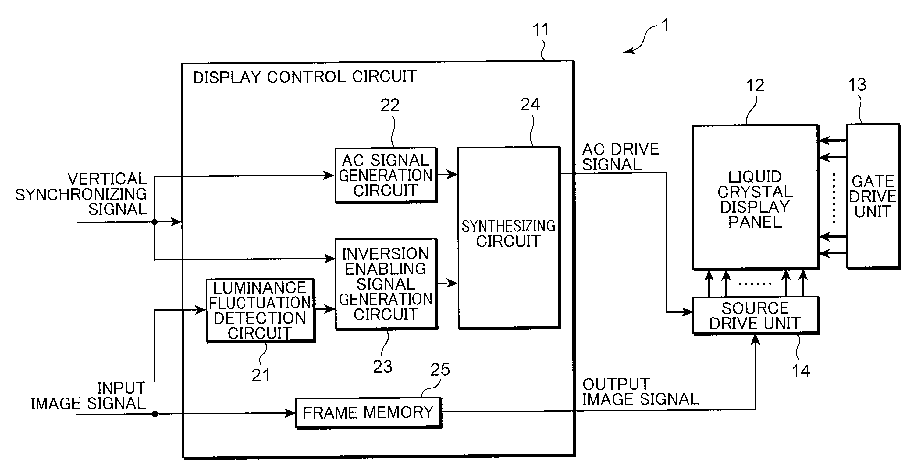
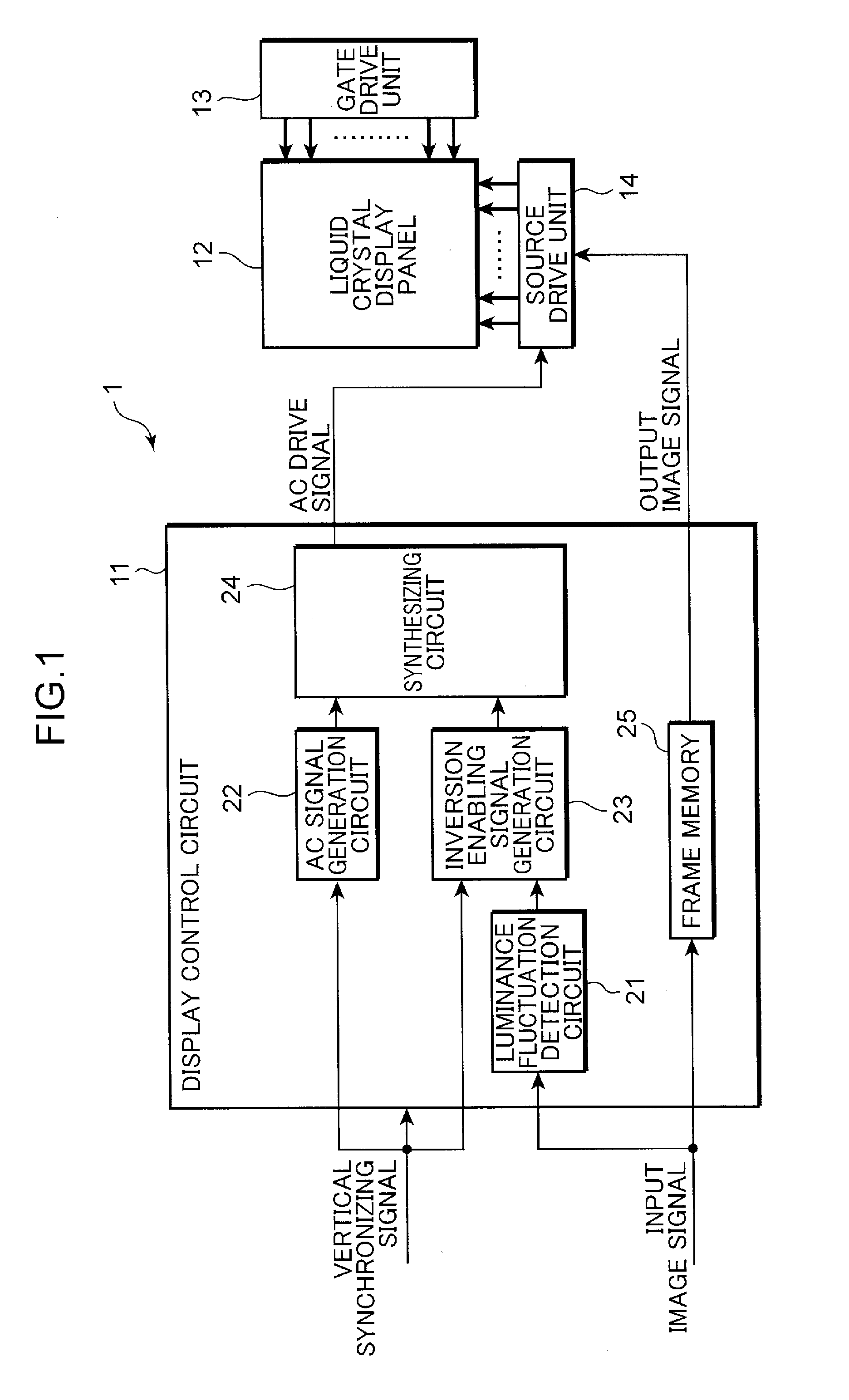
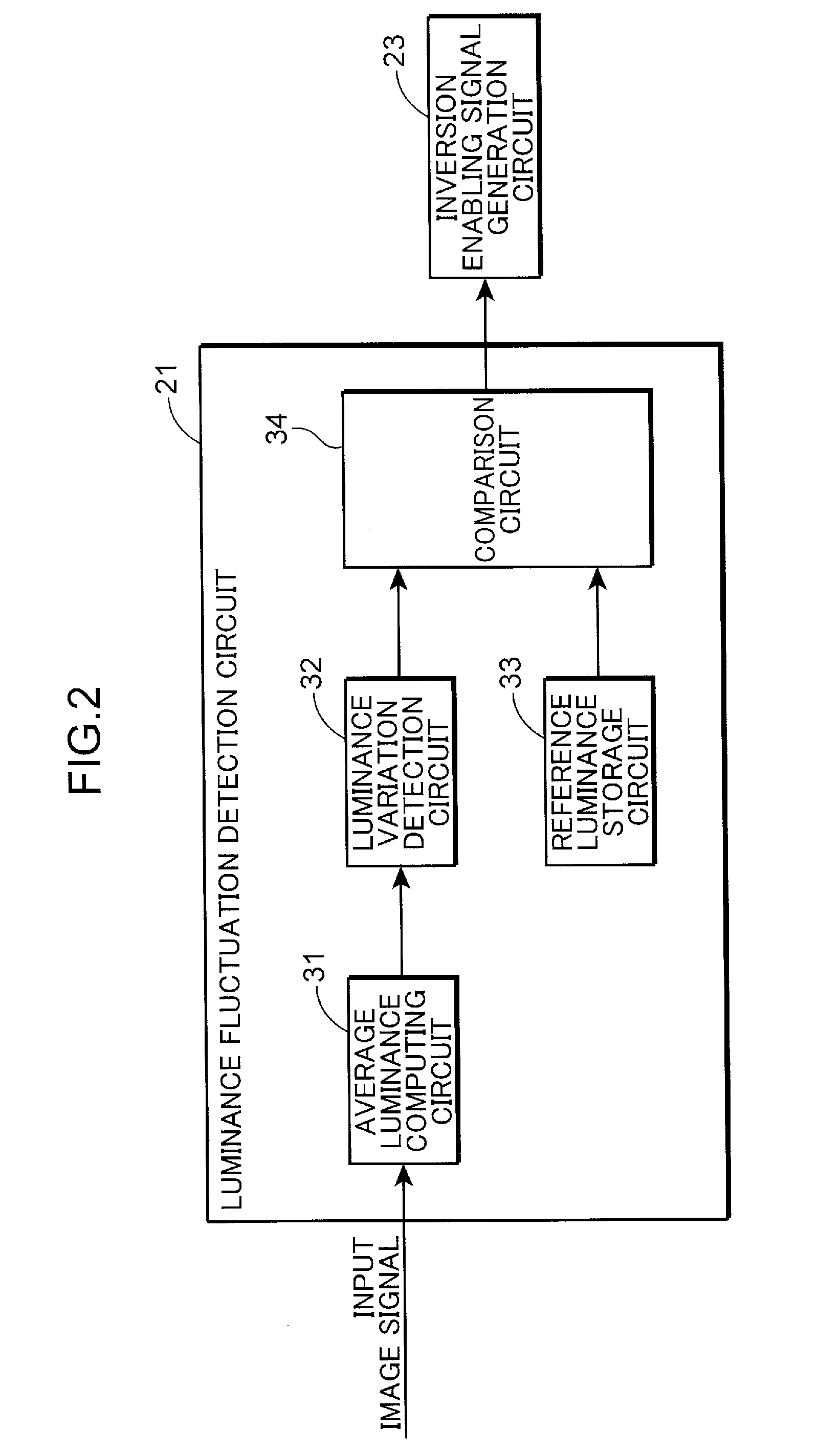
[0033]FIG. 1 is a block diagram showing a configuration of a liquid crystal display device according to a first embodiment of the instant application. FIG. 2 is a block diagram showing a configuration of a luminance fluctuation detection circuit. As shown in FIG. 1, the liquid crystal display device 1 comprises a display control circuit 11, a liquid crystal display panel 12, a gate drive unit 13, and a source drive unit 14.
[0034]The liquid crystal display panel 12 comprises the following components not shown; namely, a plurality of gate signal lines, a plurality of source signal lines and a plurality of pixels. The plurality of gate signal lines are respectively extending in a horizontal direction (main scanning direction), and provided in alignment in a vertical direction (sub scanning direction). The plurality of source signal lines are respectively extending in a vertical direction (sub scanning direction), and provided in alignment in a horizontal direction (main scanning direct...
second embodiment
[0048]FIG. 4 is a block diagram showing a configuration of a liquid crystal display device la according to a second embodiment of the instant application. In the second embodiment, the same reference numeral is given to the same element as the first embodiment, and the second embodiment is now described mainly around the differences with the first embodiment.
[0049]The liquid crystal display device la of the second embodiment shown in FIG. 4 comprises a display control circuit 11a, in substitute for the display control circuit 11, in the liquid crystal display device 1 of the first embodiment shown in FIG. 1. The display control circuit 11a additionally comprises an enabling period setting circuit 26, and additionally comprises an inversion enabling signal generation circuit 23a in substitute for the inversion enabling signal generation circuit 23 in the display control circuit 11 shown in FIG. 1.
[0050]When the high level signal is output from the comparison circuit 34 (FIG. 2) of th...
third embodiment
[0074]FIG. 8 is a block diagram showing a configuration of a liquid crystal display device 1b according to a third embodiment of the instant application. FIG. 9 is a block diagram showing a configuration of a luminance fluctuation detection circuit 21a. FIG. 10 is a diagram schematically showing a reference luminance stored in a reference luminance storage circuit 33a. In the third embodiment, the same reference numeral is given to the same element as the first and second embodiments, and the third embodiment is now described mainly around the differences with the first and second embodiments.
[0075]The liquid crystal display device 1b of the third embodiment shown in FIG. 8 comprises a display control circuit 11b, in substitute for the display control circuit 11, in the liquid crystal display device 1 of the first embodiment shown in FIG. 1. The display control circuit 11b additionally comprises an enabling period setting circuit 26a, further comprises a luminance fluctuation detect...
PUM
 Abstract
Description
Claims
Application Information


