Image-taking apparatus including a vertical transfer control device

a control device and image-taking apparatus technology, applied in the direction of radio frequency controlled devices, television system scanning details, etc., can solve the problems of uneven sensitivity, easy gain of fda, complicated control inside the ccd, etc., to achieve easy cross-wiring of the vertical transfer electrode using this area, and reduce the effect of wiring impedance and wiring width

Inactive Publication Date: 2009-01-20
FUJIFILM CORP
View PDF30 Cites 21 Cited by
  • Summary
  • Abstract
  • Description
  • Claims
  • Application Information

AI Technical Summary

Benefits of technology

[0084]If the photoelectric conversion elements are arranged according to the arrangement of the honeycomb structure, the area between the vertically and horizontally adjacent photoelectric conversion elements becomes larger than that in the case of another arrangement such as a tetragonal arrangement, and so the cross wiring of vertical transfer electrode using this area becomes easier and the wiring width does not become small. Therefore, the wiring impedance does not increase, and it is possible to curb the occurrence of unnecessary radiation, increase in power consumption and so on.
[0085]And the im

Problems solved by technology

However, there are the cases where variations in the CCD output circuits influence a generated image because no consideration is given to color filter arrangement and so on.
A Gain of the FDA is apt to have a problem such as variations appearing as uneven sensitivity.
If two CCD output circuits are provided, not only two systems of signal processing circuits for processing image-taking signals outputted from the CCD are required but control inside the CCD becomes complicated.
If the two systems of the signal processing circuits are p

Method used


Image

  • Image-taking apparatus including a vertical transfer control device
  • Image-taking apparatus including a vertical transfer control device
  • Image-taking apparatus including a vertical transfer control device

Examples


Embodiment Construction

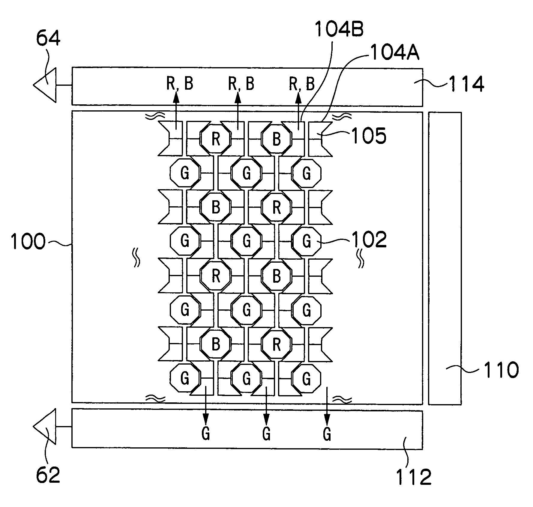
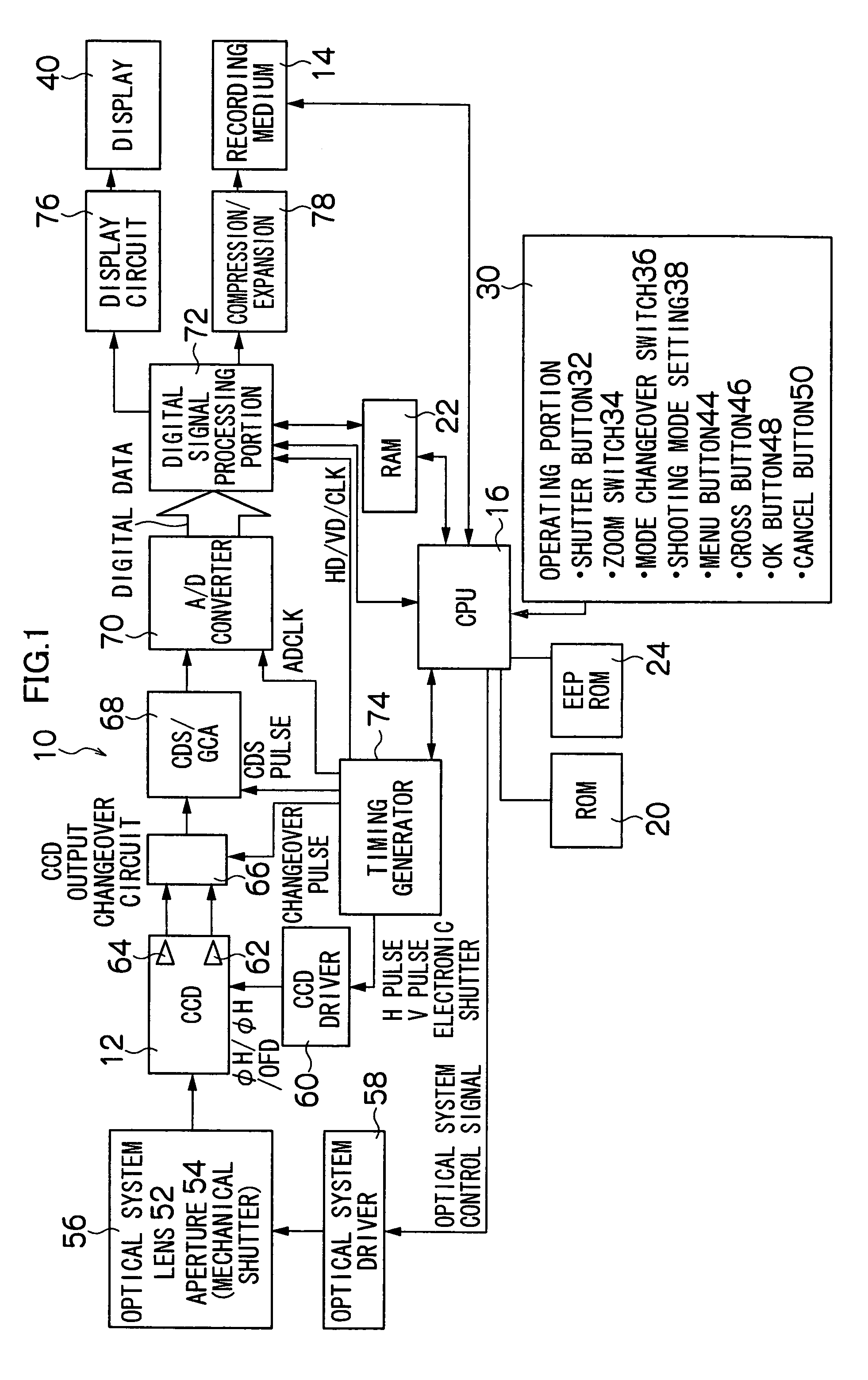
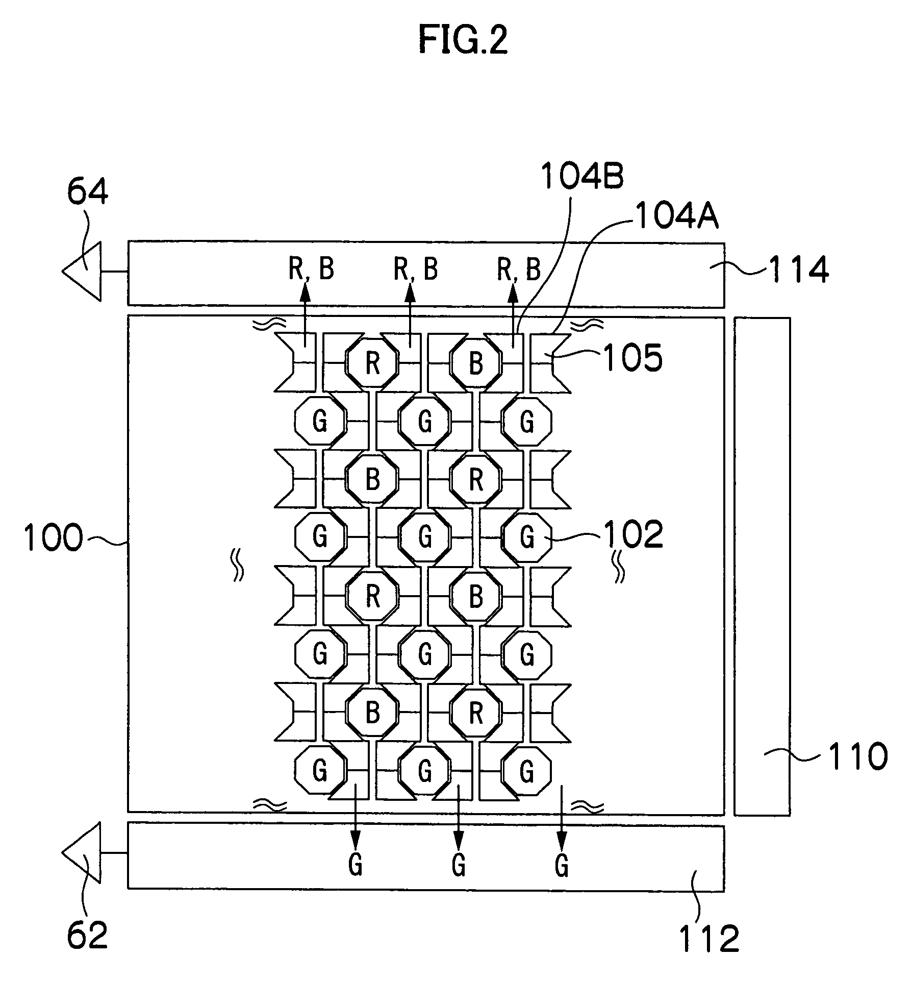
[0113]Hereafter, preferred embodiments of an image-taking apparatus and a solid-state image-taking device according to the present invention will be described according to the drawings.

[0114]FIG. 1 is a block diagram of a digital camera according to the embodiment of the present invention.

[0115]A camera 10 is the digital camera for converting an optical image of a subject taken via a CCD solid-state image-taking device (hereafter, described as a CCD) 12 to digital image data and recording it on a recording medium 14.

[0116]Operation of the entire camera 10 is integrated and controlled by a central processing unit (hereafter, described as a CPU) 16 built into the camera. The CPU 16 functions as a control device which controls this camera system according to a predetermined program, and also functions as a calculation device which performs various calculations such as an automatic exposure (AE) calculation, an automatic focusing (AF) calculation and auto white balance (AWB) control.

[01...


PUM


Abstract

An image-taking apparatus according to the present invention is constituted to have a wiring structure of transfer electrodes matching with a color filter arrangement and exert vertical transfer control over signal charges so as to transfer the signal charges read from pixels in the same color to the same horizontal transfer route. According to another embodiment of the present invention, the pixel of an image-taking device includes an odd-numbered electrode readout gate and an even-numbered electrode readout gate so that it allows control to read the charges to either of vertical transfer routes adjacent to the right and left of the pixel. It can be constituted so that one of the right and left vertical transfer routes transfers the charges to the first horizontal transfer route and the other transfers them to the second horizontal transfer route.

Description

BACKGROUND OF THE INVENTION[0001]1. Field of the Invention[0002]The present invention relates to an image-taking apparatus and a solid-state image-taking element, and in particular, to a technology for transfer control of signal charges stored in a photoelectric conversion element.[0003]2. Description of the Related Art[0004]In recent years, a CCD (Charge-Coupled Device) used for an image-taking device of a digital camera or a digital video camera is required to read and process a signal obtained from the CCD at high speed in conjunction with an increase in effective sensor resolution and a demand for high resolution. Density growth and sped-up processing of the CCD render a drive frequency thereof higher, and complexity of the CCD's structure increases wiring impedance. Consequently, various problems are arising, such as increase in unnecessary radiation, deterioration of an S / N ratio and increase in power consumption. As for moving image shooting, a readout speed of the CCD influe...

Claims


Application Information

Patent Timeline
IPC IPC(8): H04N3/14H04N5/225H04N5/335H01L27/148H04N5/365H04N5/372H04N5/376H04N5/378H04N9/04H04N9/07
CPCH04N9/045H04N23/84H04N25/134
Inventor ODA, KAZUYA
Owner FUJIFILM CORP
Why Eureka
Try Eureka