Method for production of a structure with a buried electrode by direct transfer and stucture obtained in this manner

a technology of direct transfer and buried electrodes, applied in the field of micro and nanosystems, can solve the problems of degrading mechanical properties of non-monocrystalline structural layers, thick structural layers cannot be deposited, and the structural layer cannot be monocrystalline silicon

Active Publication Date: 2013-07-11
NXP USA INC +1
View PDF18 Cites 35 Cited by
  • Summary
  • Abstract
  • Description
  • Claims
  • Application Information

AI Technical Summary

Problems solved by technology

However, in this case the structural layer cannot be monocrystalline silicon, since it is not possible to deposit monocrystalline silicon, or make it grow, on an insulating layer, or a layer of any nature other than monocrystalline silicon.
In addition, this non-monocrystalline structural layer has degraded mechanical properties compared to monocrystalline silicon.
Lastly, thick structural layers cannot be deposited due to the very lengthy treatment times, and the costly nature which results therefrom.
In addition, the problem of the stress generated by thick layers is posed, as explained in the document Ganchandani et al.
Firstly, after direct bonding and thinning, the first levels and the alignment marks are buried and therefore invisible. And it is necessary to be able to align the following levels (notably the MEMS level) with the first buried levels (notably the lower electrode). The article of Yamamoto et al mentioned above proposes to generate de...

Method used


Image

  • Method for production of a structure with a buried electrode by direct transfer and stucture obtained in this manner
  • Method for production of a structure with a buried electrode by direct transfer and stucture obtained in this manner
  • Method for production of a structure with a buried electrode by direct transfer and stucture obtained in this manner

Examples


Embodiment Construction

[0042]FIG. 1 represents a gyroscope with 2 detection elements with parallel capacitive electrodes, beneath and above the oscillating mass,

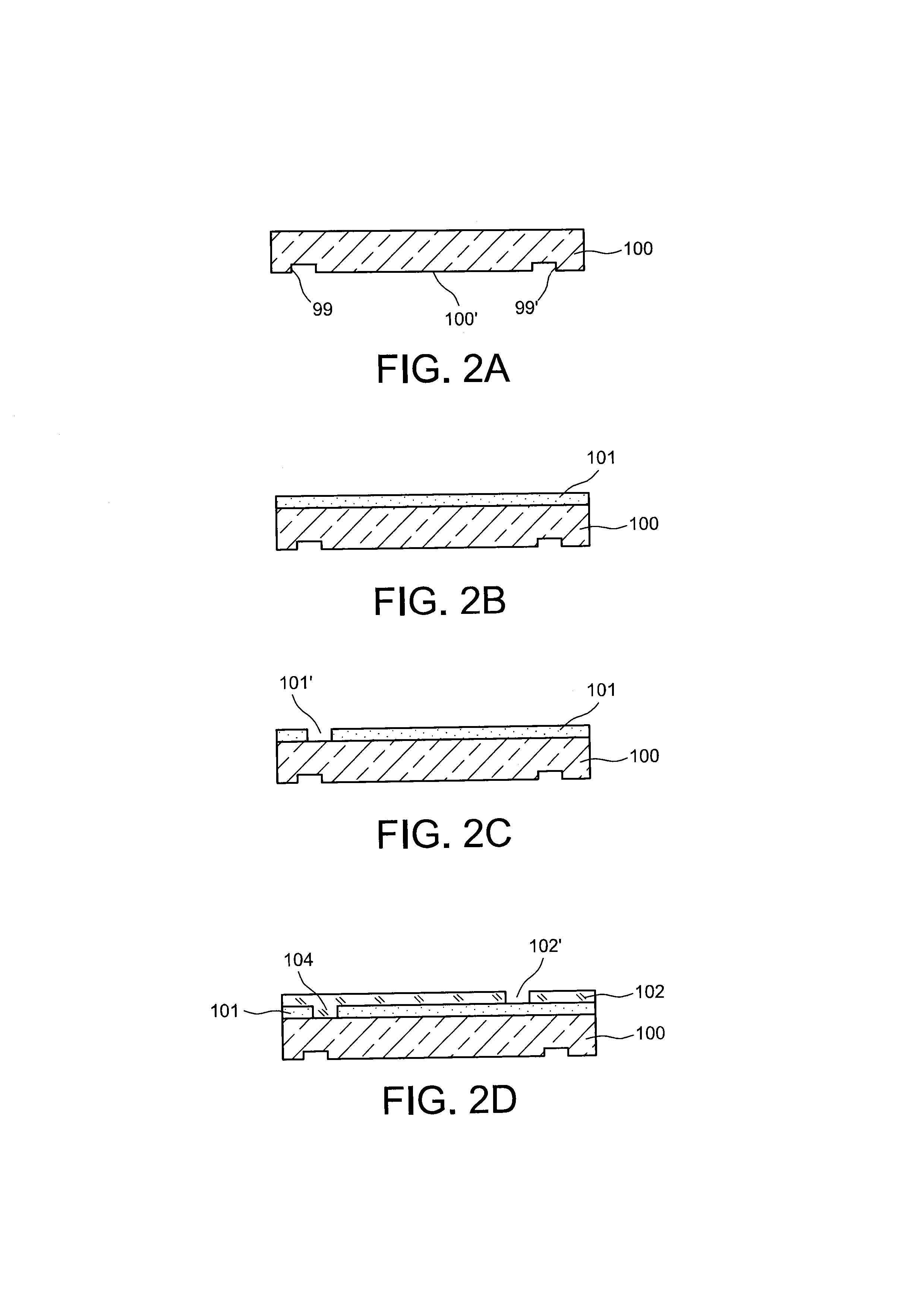
[0043]FIGS. 2A-2K represent various steps in the production of such a device,

[0044]FIGS. 3A-3G represent other steps of production of another device.

[0045]FIG. 4 represents an SOI substrate structure;

[0046]FIG. 5 represents a simplified top view of the intermediate substrate, with a moving structure;

[0047]FIG. 6 represents a system enabling substrates to be aligned.

DETAILED ACCOUNT OF PARTICULAR EMBODIMENTS

[0048]In the remainder of this document reference is made to molecular bonding, also called direct bonding or direct sealing. This assembly technique is described notably by Q. Y. Tong in “Silicon Wafer Bonding Technology for VLSI and MEMS applications”, Edited by S. S. Iyer and A. J. Auberton-Herve, 2002, INSPEC, London, Chapter 1, pages 1-20.

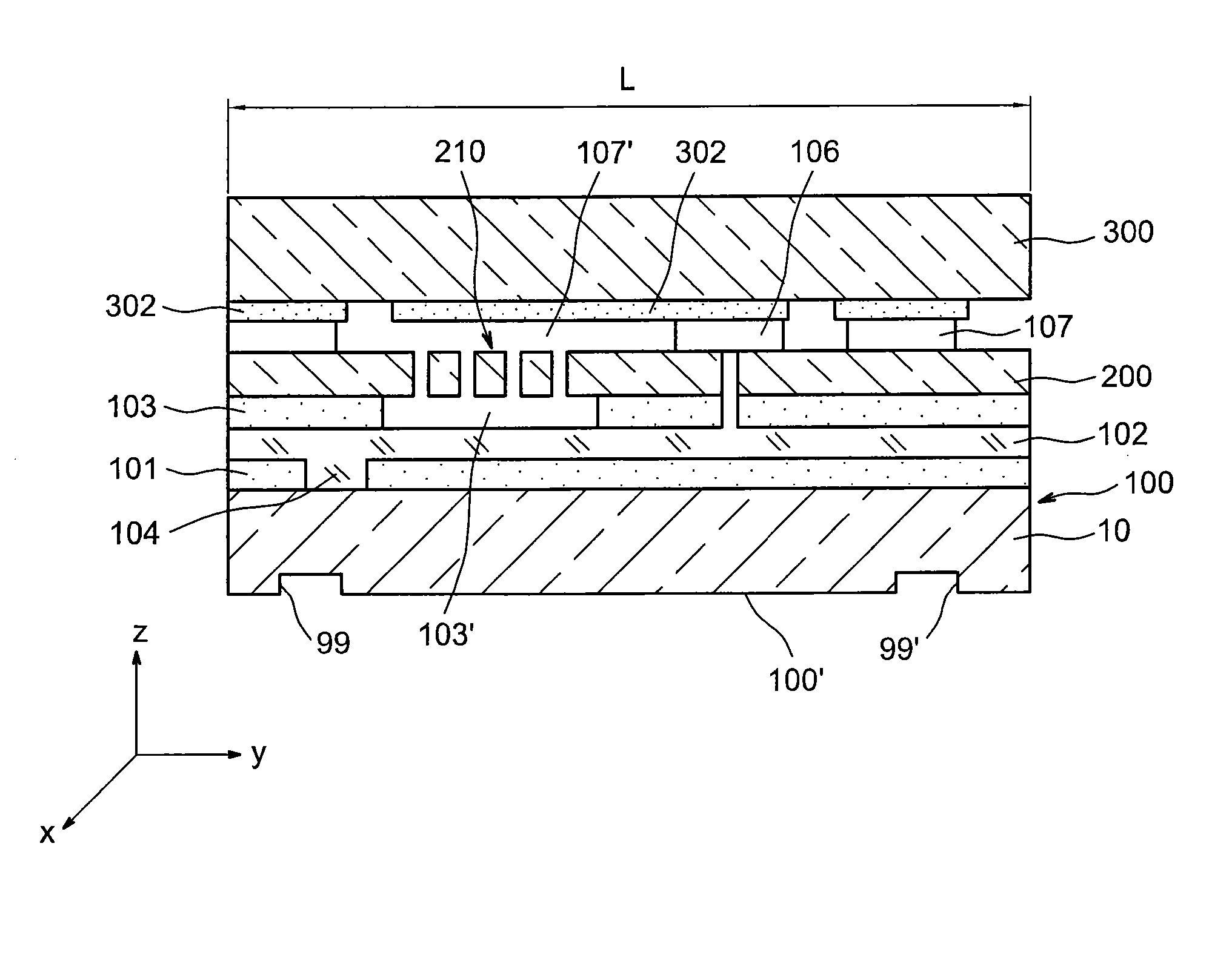
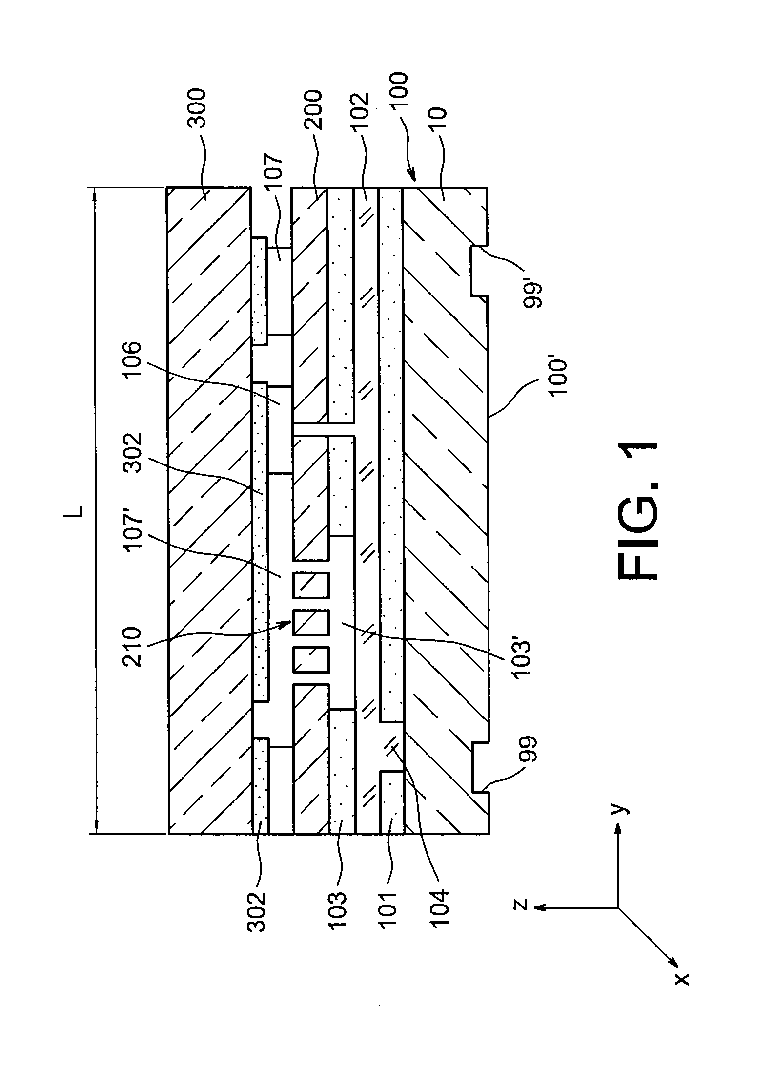
[0049]An example of a structure illustrated in FIG. 1, which is a section view, is first described.

[005...


PUM

PropertyMeasurementUnit
Semiconductor propertiesaaaaaaaaaa

Abstract

A device is described of the micro-system and/or nano-system type including:
    • a first substrate, including at least one electrode, called the lower electrode, and at least one dielectric layer,
    • an intermediate substrate, extending across a plane, called the main plane of the device, including a moving portion,
    • an upper substrate, attached to the intermediate substrate, where the said moving portion can be made to move between the lower electrode and the upper substrate.

Description

TECHNICAL FIELD AND PRIOR ART[0001]The invention concerns the field of micro- and nano-systems and their manufacture.[0002]In this type of device, moving mechanical structures are produced by selectively etching the layers of material, or sacrificial layers, which are underneath the moving structure.[0003]The invention notably enables gyroscopes to be produced, with detection elements with parallel capacitive electrodes, above and below the moving structured layer.[0004]The present invention applies more specifically to the field of micro-systems, with detection elements with capacitive electrodes parallel to the plane of the moving portion produced in a structured thin layer (for example, micro-gyroscopes).[0005]As an example of such a system, the MEMS described in document US2006 / 0208326 may be cited. In this document an AlGe hermetic metal seal is produced between two substrates. A moving MEMS structure is located in the first substrate. The second substrate (Cap) may be a CMOS w...

Claims


Application Information

Patent Timeline
IPC IPC(8): B81C1/00B81B3/00
CPCB81B2201/0235B81B2201/0242B81C3/008B81C2201/019G01P15/0802G01P15/125B81B3/00B81C1/00015G01C19/5769B81C2203/036H01L2224/83805
Inventor BERTHELOT, AUDREYLARREY, VINCENTPOLIZZI, JEAN-PHILIPPEVAUDAINE, MARIE-HELENEDESAI, HEMANTPARK, WOO TAE
Owner NXP USA INC
Why Eureka
Try Eureka