Semiconductor device

Active Publication Date: 2013-07-25
SEMICON ENERGY LAB CO LTD
View PDF5 Cites 30 Cited by
  • Summary
  • Abstract
  • Description
  • Claims
  • Application Information

AI Technical Summary

Benefits of technology

[0025]According to one embodiment of the present invention, a transistor includes an oxide semiconductor film which is etched so as to have a cross shape having different lengths in the channel length direction or to have a larger length than a source electrode and a drain electrode in the channel width direction. Thus, it is possible to reduce the probability of electrical connection between the source electrode and the drain electrode of th

Problems solved by technology

Further, the parasitic channel has caused a problem of

Method used


Image

  • Semiconductor device
  • Semiconductor device
  • Semiconductor device

Examples


embodiment 1

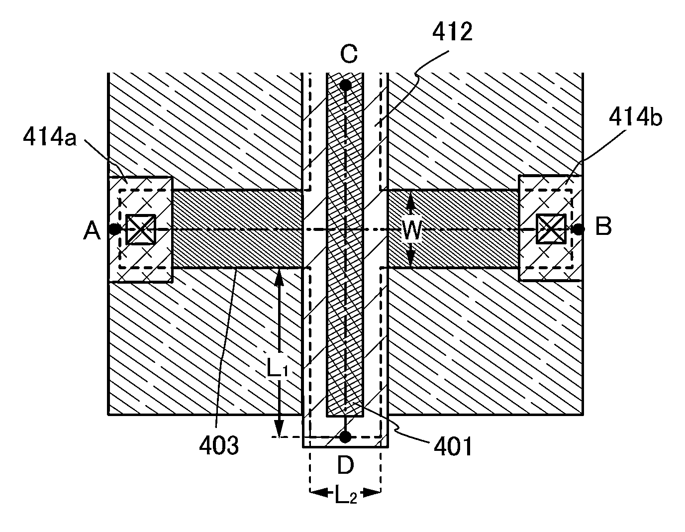
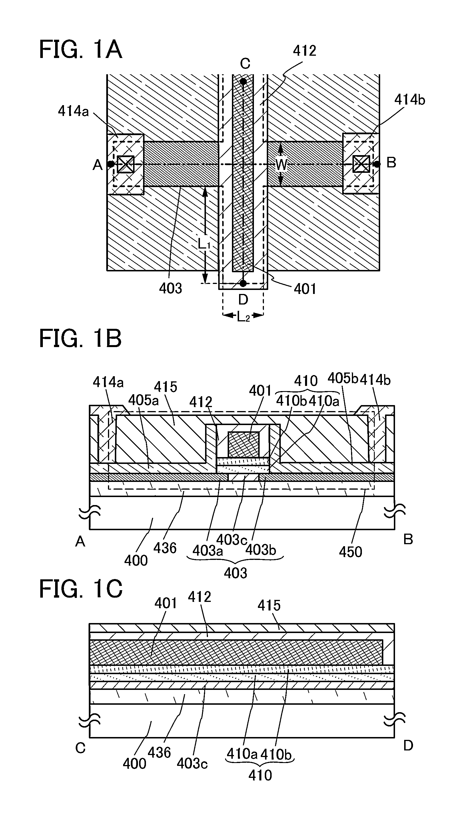
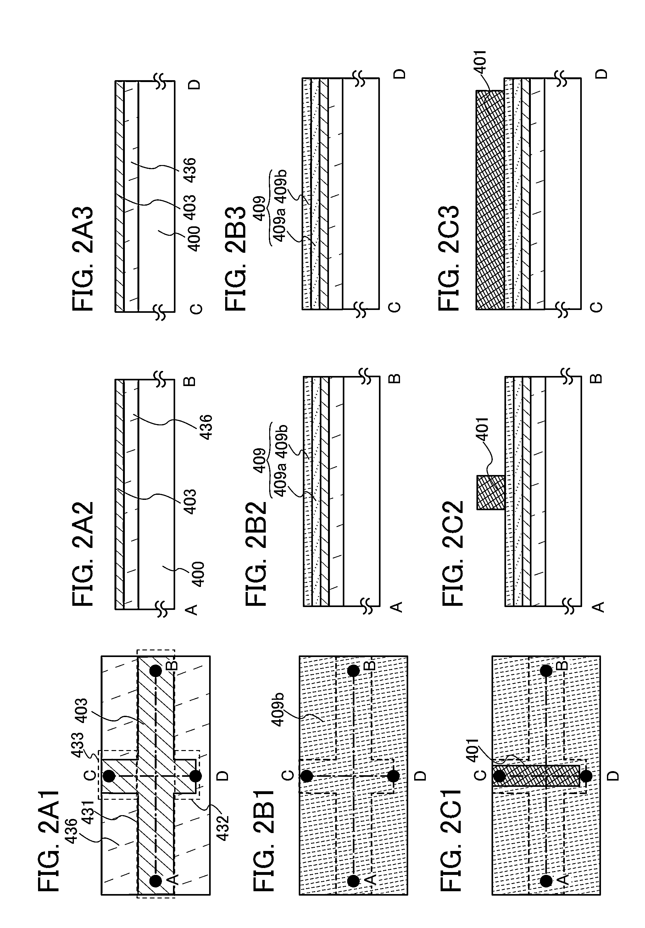
[0081]In this embodiment, one embodiment of a semiconductor device will be described with reference to FIGS. 1A to 1C. FIG. 1A is a top view of a transistor included in the semiconductor device, FIG. 1B is a cross-sectional view taken along dashed-dotted line A-B (channel length direction) in FIG. 1A, and FIG. 1C is a cross-sectional view taken along dashed-dotted line C-D in FIG. 1A. Note that some components illustrated in FIG. 1B or 1C are not illustrated in FIG. 1A for simplicity of the drawing.

[0082]A transistor 450 illustrated in FIGS. 1A to 1C includes, over a substrate 400 having an insulating surface and provided with a base insulating film 436, an oxide semiconductor film 403 including a channel formation region 403c, a source region 403a, and a drain region 403b; a gate insulating film 410; a gate electrode 401; a sidewall insulating film 412 along side surfaces and a top surface of the gate electrode 401; a source electrode 405a overlapping with the source region 403a; a...

embodiment 2

[0202]In this embodiment, another embodiment of a semiconductor device will be described with reference to FIGS. 6A to 6C. FIG. 6A is a top view of a transistor included in the semiconductor device, FIG. 6B is a cross-sectional view taken along dashed-dotted line A-B (channel length direction) in FIG. 6A, and FIG. 6C is a cross-sectional view taken along dashed-dotted line C-D in FIG. 6A. Note that some components illustrated in FIG. 6B or 6C are not illustrated in FIG. 6A for simplicity of the drawing.

[0203]A transistor 460 illustrated in FIGS. 6A to 6C includes, over the substrate 400 having an insulating surface provided with the base insulating film 436, the oxide semiconductor film 403 including the channel formation region 403c, the source region 403a, and the drain region 403b; a low-resistance region 406a; a low-resistance region 406b; the gate insulating film 410; the gate electrode 401; the sidewall insulating film 412 along a side surface of the gate electrode 401; an ins...

embodiment 3

[0243]In this embodiment, another embodiment of a semiconductor device will be described with reference to FIGS. 11A to 11C. FIG. 11A is a top view of a transistor included in the semiconductor device, FIG. 11B is a cross-sectional view taken along dashed-dotted line A-B (channel length direction) in FIG. 11A, and FIG. 11C is a cross-sectional view taken along dashed-dotted line C-D in FIG. 11A. Note that some components illustrated in FIG. 11B or 11C are not illustrated in FIG. 11A for simplicity of the drawing.

[0244]A transistor 470 illustrated in FIGS. 11A to 11C includes, over the substrate 400 having an insulating surface provided with the base insulating film 436, the oxide semiconductor film 403 including the channel formation region 403c, the source region 403a, and the drain region 403b; the source electrode 405a; the drain electrode 405b; the gate insulating film 410; the gate electrode 401; the sidewall insulating film 412 along a side surface of the gate electrode 401; t...


PUM


Abstract

Provided is a transistor which has favorable transistor characteristics and includes an oxide semiconductor, and a highly reliable semiconductor device which includes the transistor including the oxide semiconductor. In the semiconductor device including the transistor in which an oxide semiconductor film, a gate insulating film, and a gate electrode are stacked in this order, a sidewall insulating film is formed along side surfaces and a top surface of the gate electrode, and the oxide semiconductor film is subjected to etching treatment so as to have a cross shape having different lengths in the channel length direction or to have a larger length than a source electrode and a drain electrode in the channel width direction. Further, the source electrode and the drain electrode are formed in contact with the oxide semiconductor film.

Description

BACKGROUND OF THE INVENTION[0001]1. Field of the Invention[0002]The present invention relates to semiconductor devices.[0003]In this specification, a semiconductor device generally means a device which can function by utilizing semiconductor characteristics, and an electrooptic device, a semiconductor circuit, and electronic devices are all semiconductor devices.[0004]2. Description of the Related Art[0005]Attention has been focused on a technique for forming a transistor (also referred to as a thin film transistor (TFT)) using a semiconductor thin film formed over a substrate having an insulating surface. The transistor is applied to a wide range of electronic devices such as an integrated circuit (IC) or an image display device (display device). A silicon-based semiconductor material is widely known as a material for a semiconductor thin film applicable to a transistor. As another material, an oxide semiconductor has been attracting attention.[0006]For example, a transistor whose ...

Claims


Application Information

Patent Timeline
IPC IPC(8): H01L29/786
CPCH01L29/786H01L29/4908H01L27/1225H01L29/78696H01L29/7869C11C5/00F21V15/01F21V35/006F21V37/00H01L29/0657H01L29/0692H01L29/1033H01L29/24H01L29/513H01L29/518H01L29/78618
Inventor YAMAZAKI, SHUNPEI
Owner SEMICON ENERGY LAB CO LTD
Why Eureka
Try Eureka