Semiconductor storage device and method of manufacturing the same

a technology of semiconductor storage and manufacturing method, which is applied in the direction of semiconductor devices, bulk negative resistance effect devices, electrical appliances, etc., can solve the problem of serious phase-change memory problems, and achieve the effect of preventing performance deterioration

Inactive Publication Date: 2013-08-08
NAT INST OF ADVANCED IND SCI & TECH
View PDF4 Cites 36 Cited by
  • Summary
  • Abstract
  • Description
  • Claims
  • Application Information

AI Technical Summary

Benefits of technology

[0012]When the vertical transistor is in an ON state, current flows in the channel film 112 of the vertical transistor. This is because even when the phase-change film 121 is in a low-resistance state, the resistance thereof is larger than an ON resistance of the vertical transistor. When information is written in the memory cell shown in FIG. 1, the vertical transistor of a selected cell (the memory cell positioned on the lower side in FIG. 1) is turned OFF. In the selected cell where the vertical transistor is in the OFF state, current cannot flow in the channel film 112 but flows in the phase-change film 121 in a bypassing fashion. That is, the current flows along a route shown by an arrow in FIG. 1A. At this time, since Joule heat is generated in the phase-change film 121 in which current has been caused to flow, a resistance of the phase-change film 121 is changed. Therefore, by changing the magnitude of the current, operations (writing, erasing and reading) of the selected cell can be made possible.
[0013]The problem involved in the phase-change memory having such a structure lies in such a point that a resistance of a connection portion where a vertical transistor and the phase-change film 121 constituting one memory cell are connected in parallel is very high. In the phase-change memory described in the Patent Document 1, the reaction-preventing film 113 is provided between the channel film 112 and the phase-change film 121. The reaction-preventing film 113 is a film for preventing performance deterioration of the phase-change memory due to reaction of the phase-change film 121 with the channel film 112 adjacent thereto or mutual diffusion between the phase-change film 121 and the channel film 112 according to temperature rising of the phase change film 121 of the selected cell during writing operation and erasing operation of the phase-change memory, and is composed of a thin SiN film having a thickness of, for example, about 1 nm.

Problems solved by technology

However, as a result of consideration about the above-described Patent Document 1 which has been performed by the present inventors, it has been found that a serious problem is involved in the phase-change memory described in this Patent Document 1.

Method used


Image

  • Semiconductor storage device and method of manufacturing the same
  • Semiconductor storage device and method of manufacturing the same
  • Semiconductor storage device and method of manufacturing the same

Examples


Embodiment Construction

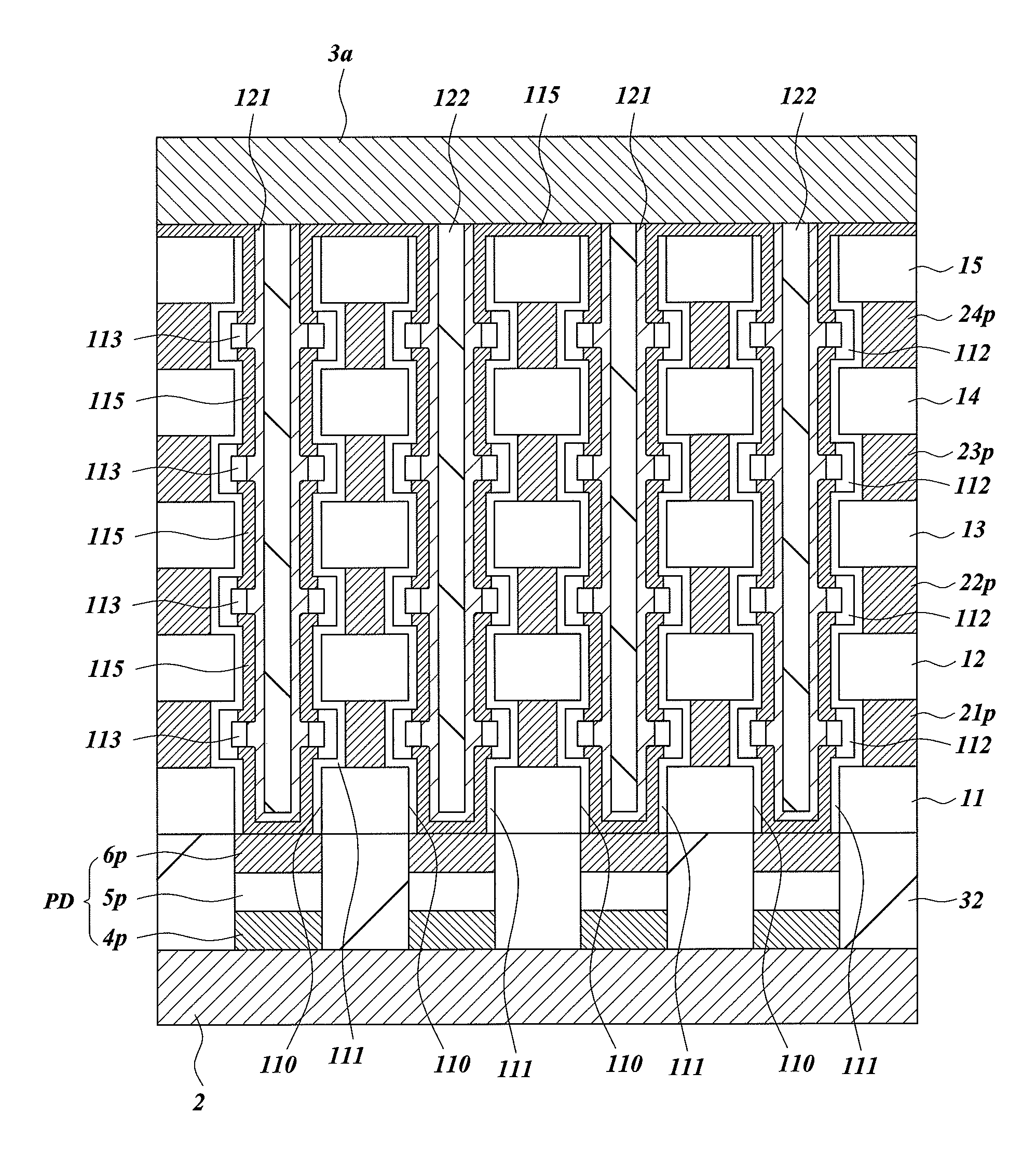
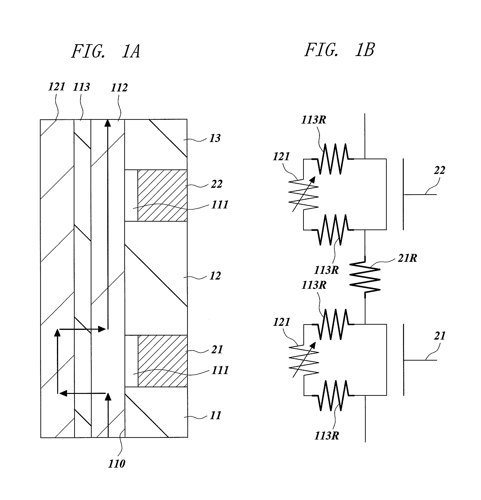
[0054]Hereinafter, an embodiment of the present invention will be described in detail with reference to the accompanying drawings. Note that components having the same function are denoted by the same reference symbols throughout the drawings for describing the embodiment, and the repetitive description thereof will be omitted. In addition, the description of the same or similar portions is not repeated in principle unless particularly required in the following embodiment. Further, in some drawings for explaining the embodiment, hatching is used even in a plan view and hatching is omitted even in a cross-sectional view so as to easily understand the configuration.

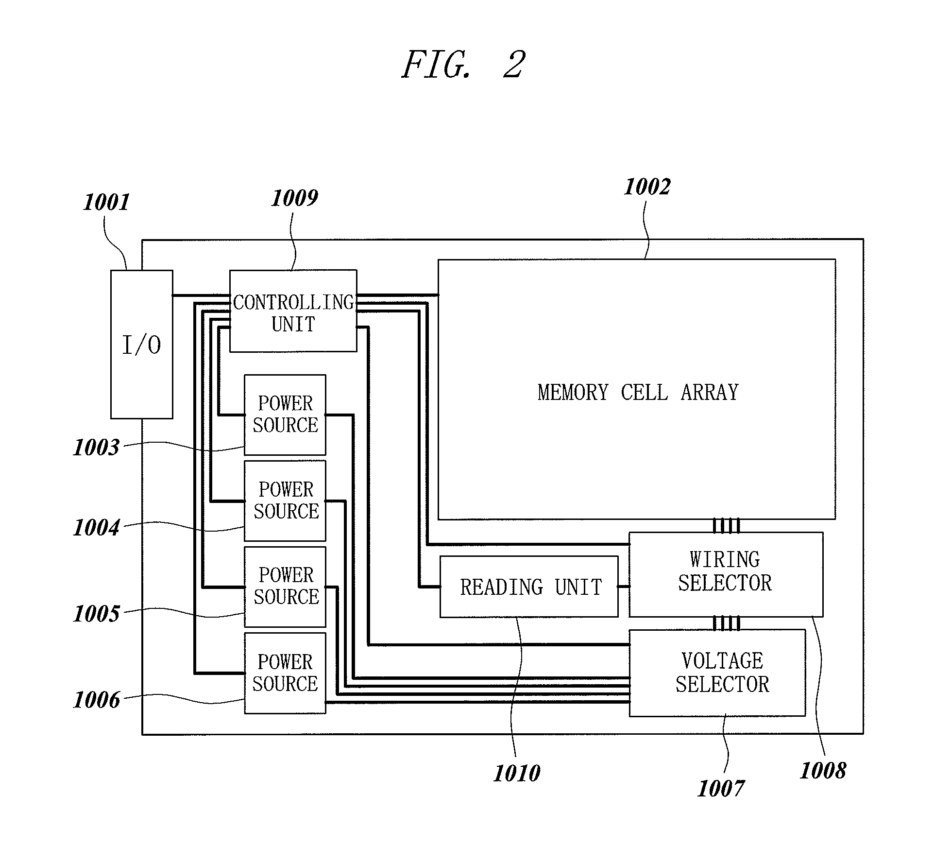
[0055]FIG. 2 is a plan view of a whole semiconductor storage device of the embodiment. As shown in FIG. 2, the semiconductor storage device according to the embodiment is provided with an I / O interface 1001 including an input and output buffer for transmission and reception of information to / from an external device (not sho...


PUM

PropertyMeasurementUnit
thicknessaaaaaaaaaa
voltageaaaaaaaaaa
voltageaaaaaaaaaa

Abstract

In a semiconductor storage device where a plurality of memory cells obtained by connecting a vertical transistor and a phase-change element in parallel is formed along a direction perpendicular to a main face of a semiconductor substrate, highly-reliable selection operation is made possible with a further low voltage. A plurality of through-holes extending through insulating films and polysilicon layers is formed in regions at which word lines and bit lines intersect with each other. A plurality of vertical chain memories composed of a gate insulating film 111, a channel film, a reaction-preventing film, a metal silicide film having a resistance lower than that of the reaction-preventing film, a phase-change film, and an embedding insulating film is formed inside each through-hole. The channel film and the reaction-preventing film are separated into respective pieces at regions among a plurality of memory cells arranged along a direction perpendicular to a main face of a semiconductor substrate. Further, the channel films of respective memory cells are connected to one another through the metal silicide films provided in regions among the plurality of memory cells.

Description

CROSS-REFERENCE TO RELATED APPLICATION[0001]The present application claims priority from Japanese Patent Application No. 2012-023345 filed on Feb. 6, 2012, the content of which is hereby incorporated by reference into this application.TECHNICAL FIELD OF THE INVENTION[0002]The present invention relates to a semiconductor storage device and a technique of manufacturing the same, and in particular to an electrically-rewritable nonvolatile semiconductor storage device that utilizes a material whose electrical characteristic changes when current is caused to flow through the material to store information, and a technique of manufacturing the same.BACKGROUND OF THE INVENTION[0003]In recent years, as a memory used instead of a flash memory that approaches the limit of miniaturization, resistance-changing type memories have been researched, and as one example of these memories, a phase-change memory using a phase-change material such as Ge2Sb2Te5 as a recording material has been researched ...

Claims


Application Information

Patent Timeline
Patent Type & Authority Applications(United States)
IPC IPC(8): H01L45/00
CPCH01L45/06H01L45/144H01L45/1608H01L27/2481H01L45/1233H01L27/2454H10B63/34H10B63/84H10N70/231H10N70/8828H10N70/826H10N70/021
Inventor MORIKAWA, TAKAHIROSHINTANI, TOSHIMICHI
Owner NAT INST OF ADVANCED IND SCI & TECH
Why Eureka
Try Eureka