Ceramic electronic component and method for producing the same

a technology of ceramic electronic components and ceramic coatings, which is applied in the manufacture of capacitors, special surfaces, capacitors, etc., can solve the problems of deterioration in reliability of moisture resistance, large thickness of resultant sintered metal films, and decrease in mechanical strength of ceramic bodies, so as to achieve superior moisture resistance and small thickness of electrode terminals.

Active Publication Date: 2013-08-08
MURATA MFG CO LTD
View PDF10 Cites 24 Cited by
  • Summary
  • Abstract
  • Description
  • Claims
  • Application Information

AI Technical Summary

Benefits of technology

[0025]In various preferred embodiments of the present invention, a ceramic electronic component can be provided wh...

Problems solved by technology

However, because the electrically conductive paste used in forming the sintered metal film has high viscosity, the thickness of the resultant sintered metal film becomes large.
In this case, a plating solution may enter the ceramic body through the site where the reaction layer is formed, which may cause a problem of a decrease in mechanical strength of the ceramic body and a problem of deterioration in reliability of moisture resistance thereof.
In addition, the high baking temperature causes the precipitation of the glass component on the surface of the sintered metal film, i.e., glass floating, which presents another problem of difficulty in forming a plating film on the surface of the sintered metal film.
Therefore, problems of a decrease in mechanical strength and deterioration in reliability of moist...

Method used


Image

  • Ceramic electronic component and method for producing the same
  • Ceramic electronic component and method for producing the same
  • Ceramic electronic component and method for producing the same

Examples


first preferred embodiment

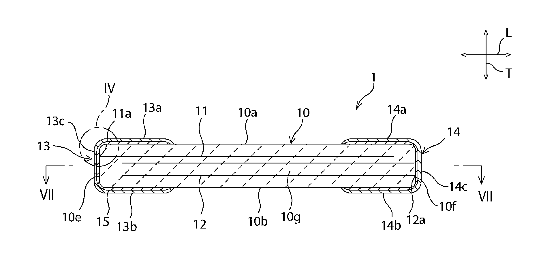
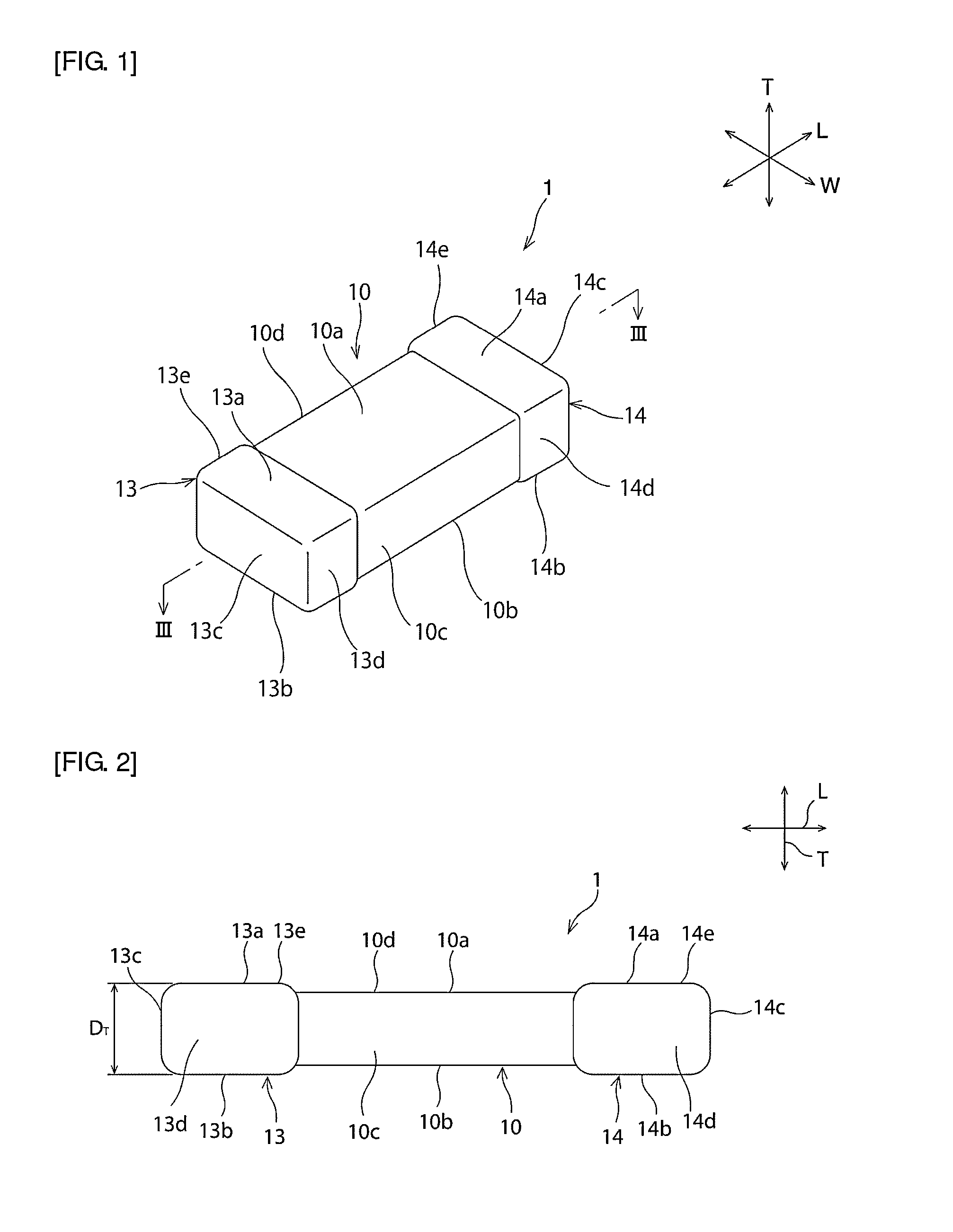
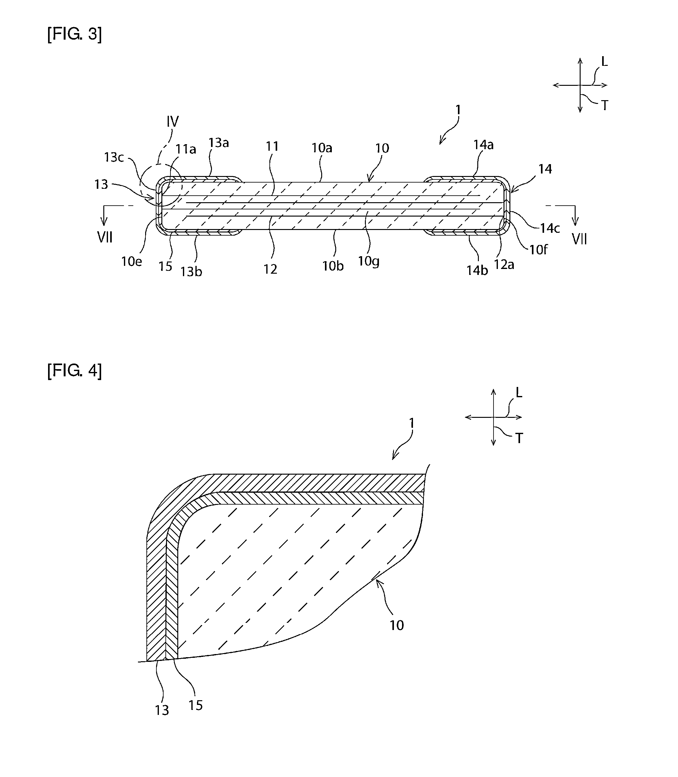
[0055]Hereinafter, preferred embodiments of the present invention will be described. However, the following preferred embodiments are merely illustrative. The present invention is not intended to be limited to the following preferred embodiments.

[0056]Throughout the drawings to which the preferred embodiments and the like refer, elements having substantially the same functions will be referred to by the same reference signs. The drawings to which the preferred embodiments and the like refer are schematically illustrated and, therefore, the dimensional ratios and the like of elements illustrated in the drawings may be different from those of the actual elements. Different drawings may have different dimensional ratios and the like of the elements. Dimensional ratios and the like of specific objects should be determined in consideration of the following descriptions.

[0057]FIG. 1 is a schematic perspective view of a ceramic electronic component according to a first preferred embodiment...

second preferred embodiment

[0159]FIG. 11 is a schematic perspective view of a ceramic electronic component according to a second preferred embodiment of the present invention.

[0160]In the above first preferred embodiment, an example has been described in which the first and second electrode terminals 13 and 14 and the glass coating layers 15 are preferably located on the first and second side surfaces 10c and 10d. However, as shown in FIG. 11, the first and second electrode terminals 13 and the glass coating layers 15 may not be substantially provided on the first and second side surfaces 10c and 10d.

[0161]The ceramic electronic component according to the second preferred embodiment can be produced, for example, in the following manner. A mother laminate 22 (see FIG. 12) is obtained in the same manner as in the method for producing the ceramic electronic component 1 according to the first preferred embodiment. In this preferred embodiment, next, as shown in FIG. 12, an electrically conductive pattern 23 havi...

third preferred embodiment

[0164]FIG. 13 is a schematic cross-sectional view of a ceramic electronic component according to a third preferred embodiment of the present invention.

[0165]In the above first preferred embodiment, an example has been described in which the first and second electrode terminals 13 and 14 and the glass coating layers 15 are preferably located on both the first and second principal surfaces 10a and 10b. However, the present invention is not limited to this configuration. The first and second electrode terminals 13 and the glass coating layers 15 only have to be located somewhere on the surface of the ceramic body 10.

[0166]For example, as shown in FIG. 13, the first and second electrode terminals 13 and 14 and the glass coating layers 15 may be provided on the second principal surface 10b but not provided on the first principal surface 10a.


PUM


Abstract

A ceramic electronic component includes a ceramic body, a glass coating layer, and an electrode terminal. The ceramic body includes a plurality of internal electrodes whose ends are exposed on the surface of the ceramic body. The glass coating layer covers a portion of the ceramic body on which the internal electrodes are exposed. The electrode terminal is provided directly on the glass coating layer. The electrode terminal includes a plating film. The glass coating layer is made of a glass medium in which metal powder particles are dispersed. The metal powder particles define conduction paths that electrically connect the internal electrodes with the electrode terminal.

Description

BACKGROUND OF THE INVENTION[0001]1. Field of the Invention[0002]The present invention relates to a ceramic electronic component and a method for producing the same.[0003]2. Description of the Related Art[0004]Ceramic electronic components, typified by ceramic capacitors, are widely used in electronic devices, such as a cellular phone or a portable audio player. A ceramic electronic component generally includes a ceramic body; internal electrodes whose ends are exposed on the surface of the ceramic body; and external electrodes disposed to cover the surface regions of the ceramic body on which the internal electrodes are exposed. Examples of the external electrode include one obtained by applying and baking an electrically conductive paste on the ceramic body to form a sintered metal film and then plating the sintered metal film, as described in JP-A-2002-203737, and one formed only of a plating film, as described in JP-A-2004-327983.[0005]However, because the electrically conductive...

Claims


Application Information

Patent Timeline
IPC IPC(8): H01G13/00H01G4/30
CPCH01G4/30H01G4/306H01G13/006H01G4/2325
Inventor NISHISAKA, YASUHIROSANADA, YUKIOKISUMI, TETSUYANAGAMOTO, TOSHIKIKIMURA, MASATOKOGA, SEIJI
Owner MURATA MFG CO LTD
Why Eureka
Try Eureka