
Volatile Memory with a Decreased Consumption

a volatile memory and consumption technology, applied in the field of integrated circuits, can solve the problems of critical factors such as consumption of the integrated circuit comprising a volatile memory, data stored in the memory cells is at risk of being lost, and memory is called volatil

Inactive Publication Date: 2013-08-08
STMICROELECTRONICS SRL
View PDF5 Cites 1 Cited by
  • Summary
  • Abstract
  • Description
  • Claims
  • Application Information

AI Technical Summary

Benefits of technology

The patent describes a type of memory that uses less power and has smaller parasitic currents in both read and write operations. The memory has separate memory cells for each row, and each group of cells has its own selection circuit for writing and reading. The selection circuits have MOS transistors and switches to connect to the memory cells. The memory also has read bit lines and write word lines for each column, and some of the MOS transistors can connect to both read and write bit lines. The electronic device containing this memory can be powered by a battery. A method is also provided for accessing data stored in the memory.

Problems solved by technology

A memory is called volatile in the case where the data stored in the memory cells risk being lost when the memory power supply voltage falls below a minimum threshold.
For certain applications, the consumption of the integrated circuit comprising a volatile memory is a critical factor.
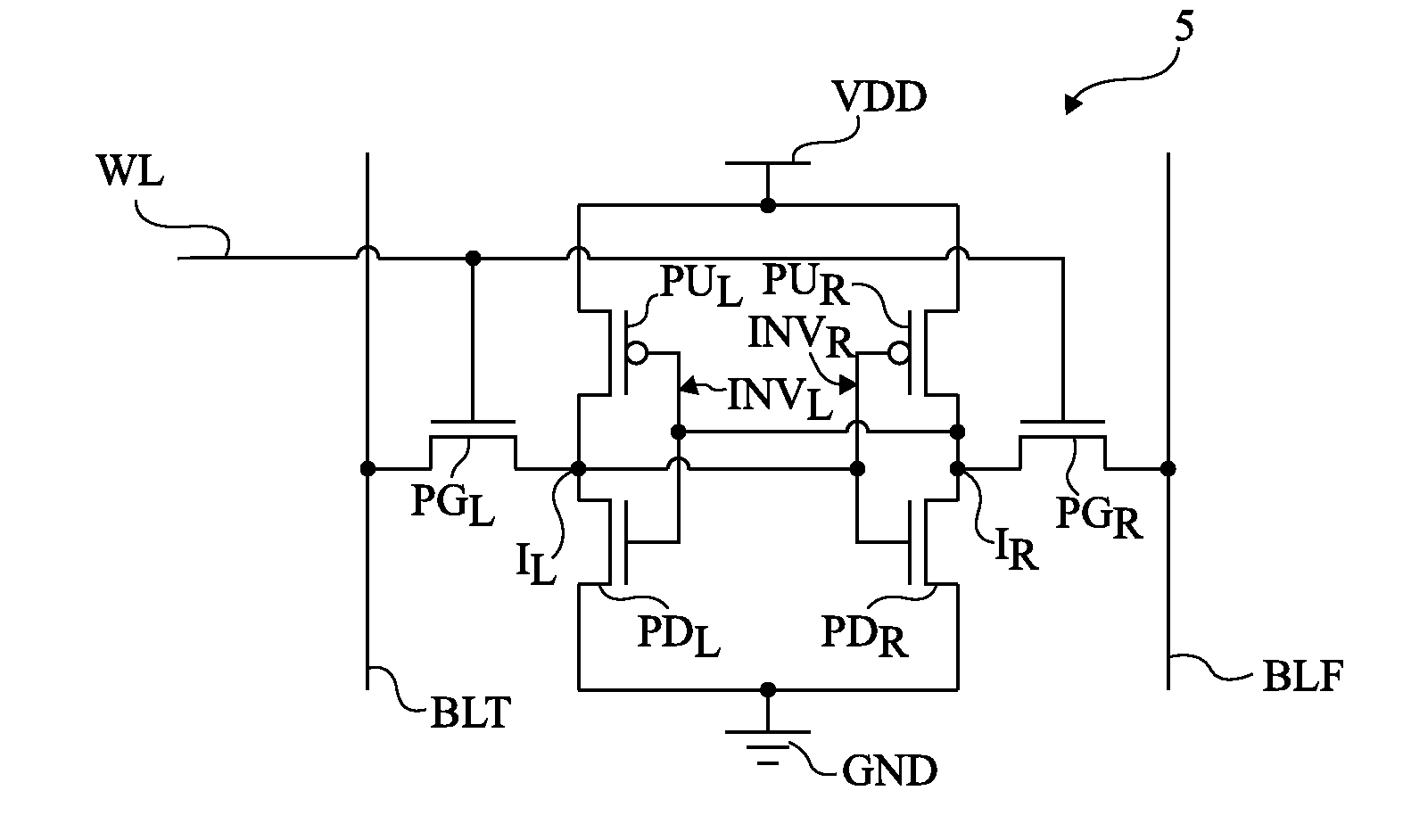
However, the decrease of the power supply voltage may cause read errors in an operation of reading of the datum stored in memory cell 5.
However, even if switches PGL and PGR of all the other memory cells of the column are on, leakage currents may flow for these memory cells through some of switches PGL and PGR.
With the decrease of power supply voltage VDD, the total leakage current corresponding to the sum of the leakage currents of the unselected memory cells of the column may cause incorrect variations of the voltages of bit lines BLT and BLF and thus read errors.

Method used


Image

  • Volatile Memory with a Decreased Consumption
  • Volatile Memory with a Decreased Consumption
  • Volatile Memory with a Decreased Consumption

Examples


Embodiment Construction

[0046]For clarity, the same elements have been designated with the same reference numerals in the different drawings. In the following description, expression “conduction terminal” of a MOS transistor indifferently designates the MOS transistor source or drain.

[0047]The memory cells according to the embodiments described hereinafter may be powered at a decreased power supply voltage VDD. As an example, voltage VDD may be on the order of 400 mV, especially when the memory cells are formed in a technology for which the channel length of MOS transistors is 32 nm. In particular, the memory cells according to the embodiments described hereinafter are capable of operating under the MOS transistor threshold voltage.

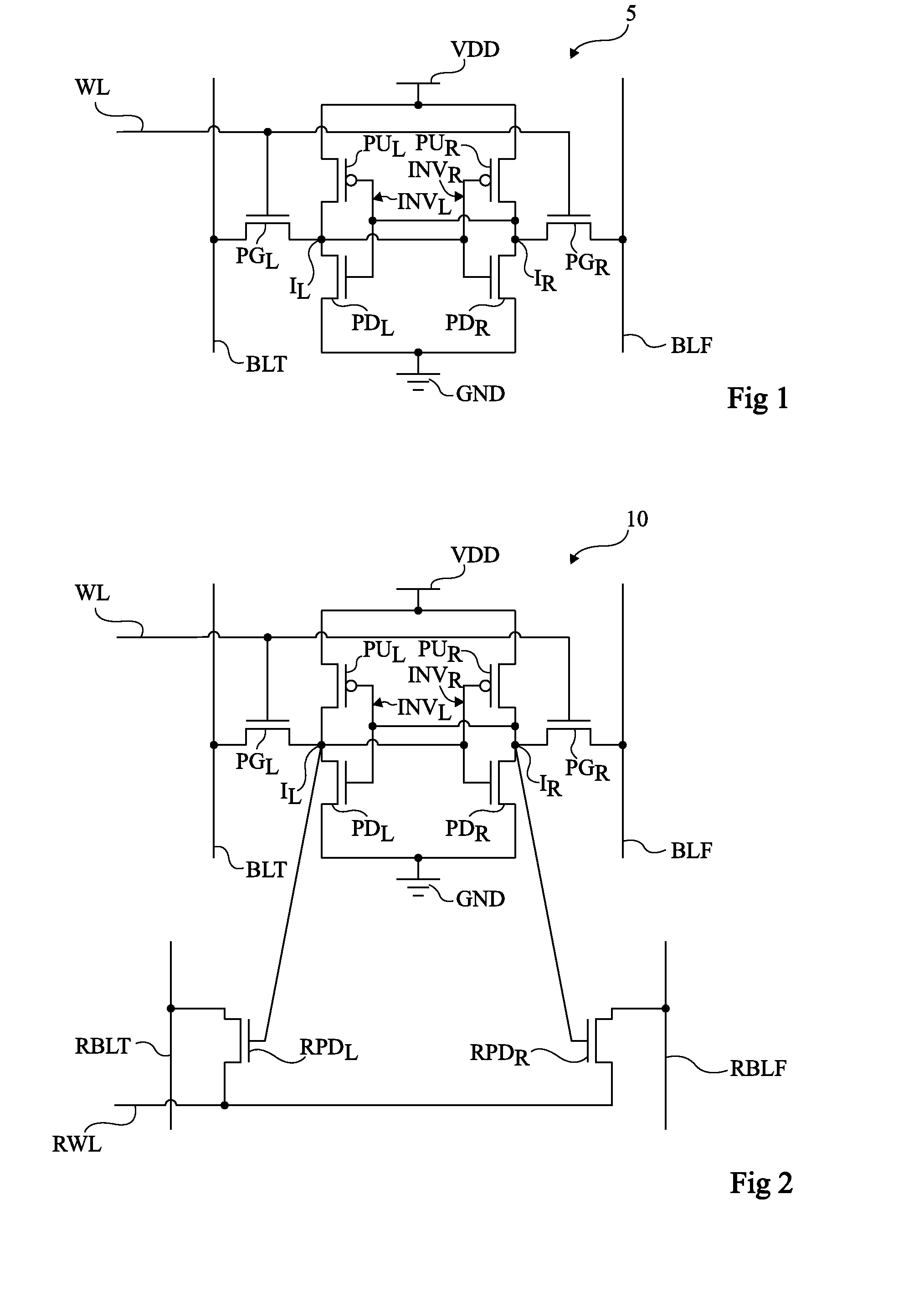
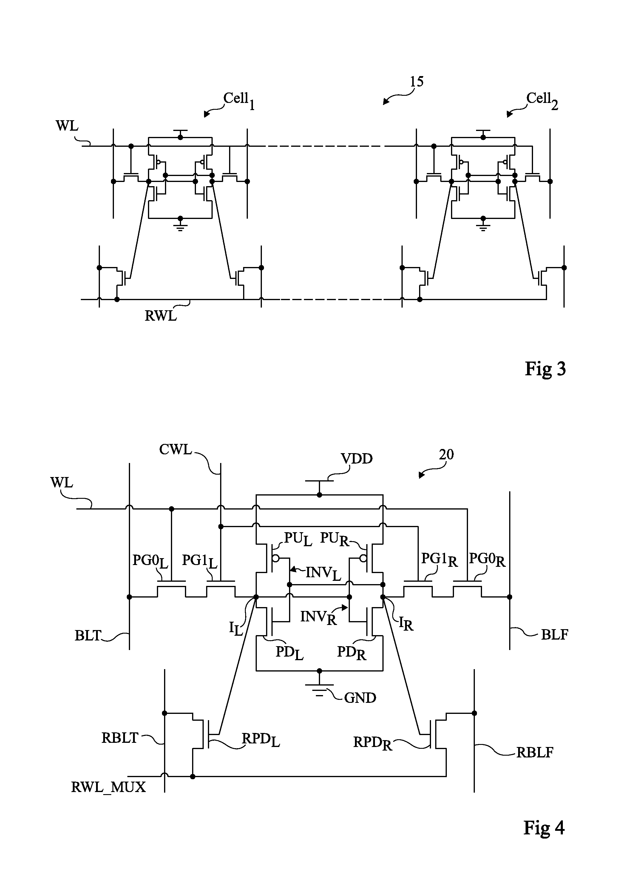
[0048]FIG. 4 shows an embodiment of a volatile memory cell 20. As compared with memory cell 10 shown in FIG. 2, memory cell 20 comprises two additional MOS transistors. Transistor PGL of memory cell 10 is replaced with two N-type MOS transistors, PG0L and PG1L. The gate of trans...


PUM


Abstract

A volatile memory including volatile memory cells adapted to the performing of data write and read operations. The memory cells are arranged in rows and in columns and, further, are distributed in separate groups of memory cells for each row. The memory includes a first memory cell selection circuit configured to perform write operations and a second memory cell selection circuit, different from the first circuit, configured to perform read operations. The first circuit is capable of selecting, for each row, memory cells from one of the group of memory cells for a write operation. The second circuit is capable of selecting, for each row, memory cells from one of the groups of memory cells for a read operation.

Description

CROSS-REFERENCE TO RELATED APPLICATIONS[0001]This application claims the priority benefit of French patent application number 12 / 51036, filed on Feb. 3, 2012, which is hereby incorporated by reference to the maximum extent allowable by law.TECHNICAL FIELD[0002]The present disclosure relates to integrated circuits comprising volatile memory elements.BACKGROUND[0003]An integrated circuit memory may be formed of an assembly of memory elements, or memory cells, which may be arranged in an array. The data writing into and reading from memory cells are performed by means of dedicated logic circuits. A power supply generally provides the power necessary to the proper operation of the memory cell components and of the logic circuit. The memory power supply is generally obtained by one or several rails connected to all the memory cells and transmitting a power supply voltage. A memory is called volatile in the case where the data stored in the memory cells risk being lost when the memory pow...

Claims


Application Information

Patent Timeline
Patent Type & Authority Applications(United States)
IPC IPC(8): G11C7/00
CPCG11C7/00G11C8/12G11C8/14G11C11/419G11C14/0054G11C8/00G11C13/0069G11C8/16
Inventor FEKI, ANISLAFONT, JEAN-CHRISTOPHETURGIS, DAVID
Owner STMICROELECTRONICS SRL
Learn More