
Semiconductor device and method of generating sense signal

a technology of sensing signal and semiconductor device, which is applied in the direction of static storage, digital storage, instruments, etc., can solve the problems of limitation on the reduction of data line voltage datab, difficulty in raising power supply voltage vcc, etc., and achieves the effect of easy circuit matching and low power supply voltag

Active Publication Date: 2006-02-02
MONTEREY RES LLC
View PDF9 Cites 9 Cited by
  • Summary
  • Abstract
  • Description
  • Claims
  • Application Information

AI Technical Summary

Benefits of technology

[0016] According to the present invention, the second potential generated by the difference between the core cell current and the reference current makes it possible to handle the voltage that swings in the full range of a power supply potential and the ground potential and to efficiently utilize the amplitude range of the power supply voltage. It is thus possible to improve the effective sensing precision. That is, the sensing is enabled for a fine current margin. Further, the first potential is generated without being affected by the second cascode circuit, and the first and second cascode circuits can easily be matched. The present invention provides the semiconductor device equipped with the high-precision cascode circuits in which the matching between the cascode circuits can easily be made.
[0028] According to the present invention, there is provided a semiconductor device with a high-precision cascode circuit capable of easily making a circuit match and operating with a low power supply voltage.

Problems solved by technology

Thus, there is a difficulty in raising the power supply voltage VCC.
Therefore, there is a limitation on reduction of the data line voltage DATAB within the range in which a sufficiently responsible current is ensured during the sensing period.

Method used


Image

  • Semiconductor device and method of generating sense signal
  • Semiconductor device and method of generating sense signal
  • Semiconductor device and method of generating sense signal

Examples


first embodiment

[0040]FIG. 3 shows a semiconductor device according to a first embodiment of the present invention. A semiconductor device 10 includes a cascode circuit (SAR) 20 for a reference cell, a plurality of cascode circuits (CAS) 30 for core cells, and a plurality of sense amplifiers (S / A) 40. The semiconductor device 10 may be a semiconductor memory device solely packaged like a flash memory, or may be incorporated into a semiconductor device as a part therein, such as a system LSI.

[0041]FIG. 3 shows a circuit configuration for reading an SLC (Single Level Cell). In SLC, cell data is read with the single reference cell. Thus, the cascode circuit 20 for the reference cell is prepared. The reference cell is connected to the drain terminal of the reference cell through a data line DATABref. The cascode circuit 20 for the reference cell generates a reference voltage Saref and an NMOS gate voltage NG.

[0042] Further, 16 cascode circuits 30 for core cells are provided and connected, via data li...

second embodiment

[0052] Now, a second embodiment will be described. FIG. 6 shows a relationship between the core cell current and the reference current in reading an MLC (two bits / cell). The MLC is configured so that the memory cell has different threshold values. In FIG. 6, the horizontal axis denotes the gate voltage (threshold value for the distribution of threshold values), and the vertical axis denotes the drain current (the degree of distribution for the distribution of threshold values). The threshold values of the cell define two bits and fall in any of states “0”, “1”, “2” and “3”.

[0053] By way of example, a case is considered where a core cell having a threshold value of LEVEL1 is selected and read. A word line WL voltage used at the time of reading is applied to the gate electrodes of three reference cells ref(2:0) and the selected core cell. The word line voltage is set at a level at which little current flows through a core cell having a threshold value of LEVEL3. At that time, the cel...

third embodiment

[0065] The third embodiment of the present invention will now be described. When it takes a long time to charge the data line DATAB, a current for charging the data line flows the PMOS transistors of the PMOS current mirror in addition to the current of the cell selected during the sense period. This reduces the margin for sensing of the cells through which the currents do not flow. The cascode circuit employed in the third embodiment shown in FIG. 9 is designed to avoid the above problem.

[0066]FIG. 9 shows the cascode circuit for the core cell employed in the third embodiment. A core cell cascode circuit 230 includes transistors 233 and 234, a PMOS current mirror, resistors 237 through 239, a PMOS transistor 240, an NMOS transistor 241, and an inverter 242. The transistors 233 and 234 are cascode-connected to a data line 231 of the core cell. The PMOS current mirror is composed of PMOS transistors 235 and 236. The PMOS transistor 240, the NMOS transistor 241 and the inverter 242 f...


PUM


Abstract

A semiconductor device includes a first cascode circuit having a first current mirror amplifying a reference current flowing through a data line of a reference cell, and a second current mirror generating a first potential from an amplified reference current; and a second cascode circuit having a third current mirror amplifying a core current flowing through a data line of a core cell, and a transistor receiving a gate voltage corresponding to the amplified reference current and generating a second potential based on a difference between an amplified core cell current and the amplified reference current. Since the second potential is generated by the difference between the core cell current and the reference cell current, the second potential swings in the full range of the ground power supply voltage to the ground potential, and the range of the amplitude of the power supply voltage can be efficiently utilized. Sensing is enabled for a fine current margin.

Description

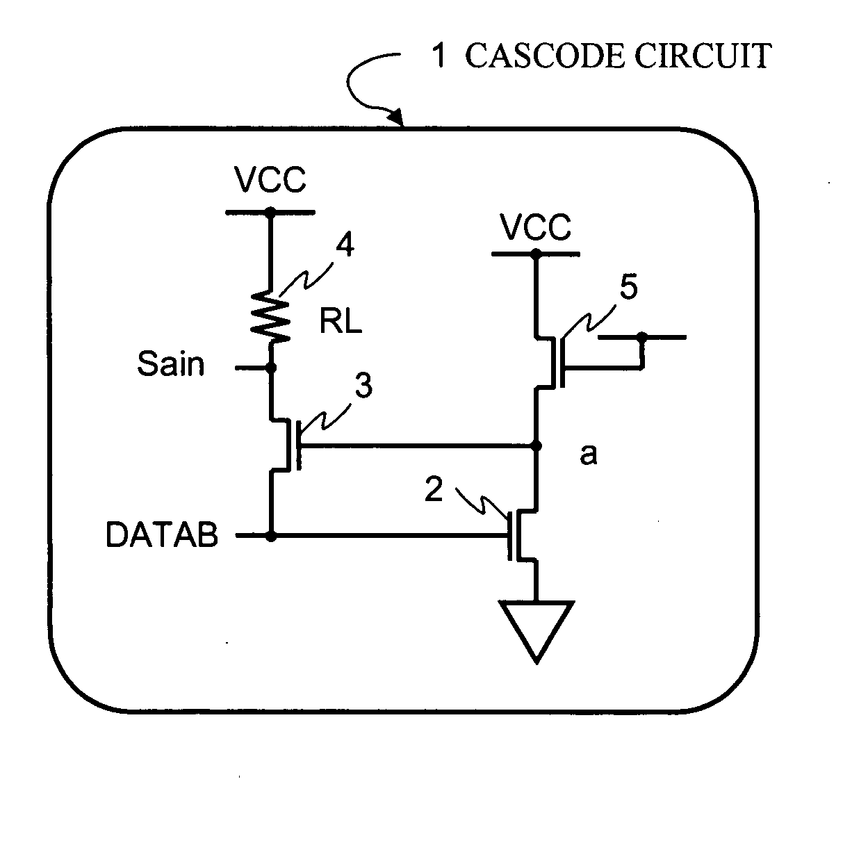
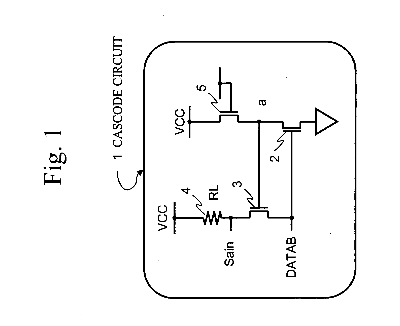
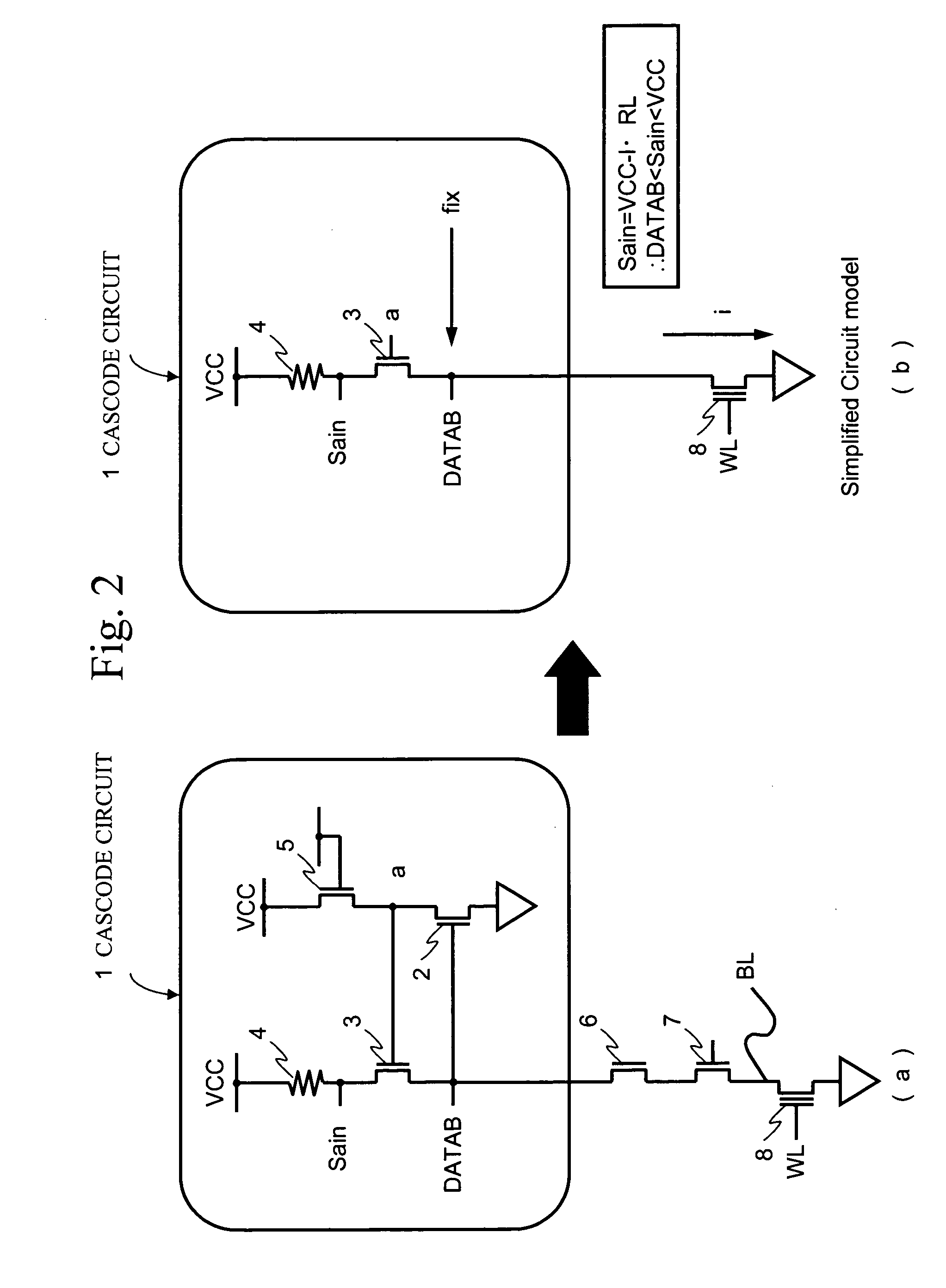
CROSS REFERENCE TO RELATED APPLICATIONS [0001] This is a continuation of International Application No. PCT / JP2004 / 010915, filed Jul. 30, 2004.BACKGROUND OF THE INVENTION [0002] 1. Field of the Invention [0003] The present invention relates to a semiconductor device and a method of generating a sense signal, and more particularly, to a semiconductor device with a high-precision cascode connection and a method of generating a sense signal. [0004] 2. Description of the Related Art [0005] Semiconductor memories are categorized into a volatile type in which information is lost by power off and a non-volatile type in which information is retained even by power off. The latter type of semiconductor memory is typically a flash memory in which data can be erased on a given-area basis with a reduced rewriting time. A cascode circuit is employed to implement the current-to-voltage conversion in the flash memories. [0006]FIG. 1 is a diagram of a conventional cascode circuit. Referring to FIG. 1...

Claims


Application Information

Patent Timeline
Patent Type & Authority Applications(United States)
IPC IPC(8): G11C7/02
CPCG11C7/062G11C7/067G11C2211/5645G11C16/28G11C11/5642G11C16/30G11C16/26
Inventor NAKAI, TSUTOMUAKAOGI, TAKAOKUROSAKI, KAZUHIDE
Owner MONTEREY RES LLC
Learn More