Oscillator and IC chip

Active Publication Date: 2013-12-19
ASAHI KASEI ELECTRONICS CO LTD
View PDF3 Cites 5 Cited by
  • Summary
  • Abstract
  • Description
  • Claims
  • Application Information

AI Technical Summary

Benefits of technology

The patent text is saying that it's possible to reduce the power supply voltage without affecting the quality of the signal, using the same circuit design as before. This means that it's possible to lower the power supply voltage without compromising the performance of the circuit.

Problems solved by technology

In such a circuit configuration of the conventional oscillator described in Patent document 1, however, lowering of the voltage cannot be expected drastically, even if the power supply voltage is attempted to be lowered.
Besides, in the circuit configuration of the conventional oscillator, even if the power supply voltage is merely lowered, the dynamic range will be narrower and the phase noise may degrade.
For this reason, in the circuit configuration of the conventional oscillator, it is difficult to lower the power supply voltage.
Further, such a problem is found at not only the crystal oscillator with a crystal oscillation unit but also an oscillation circuit with another oscillation device.

Method used


Image

  • Oscillator and IC chip
  • Oscillator and IC chip
  • Oscillator and IC chip

Examples


first embodiment

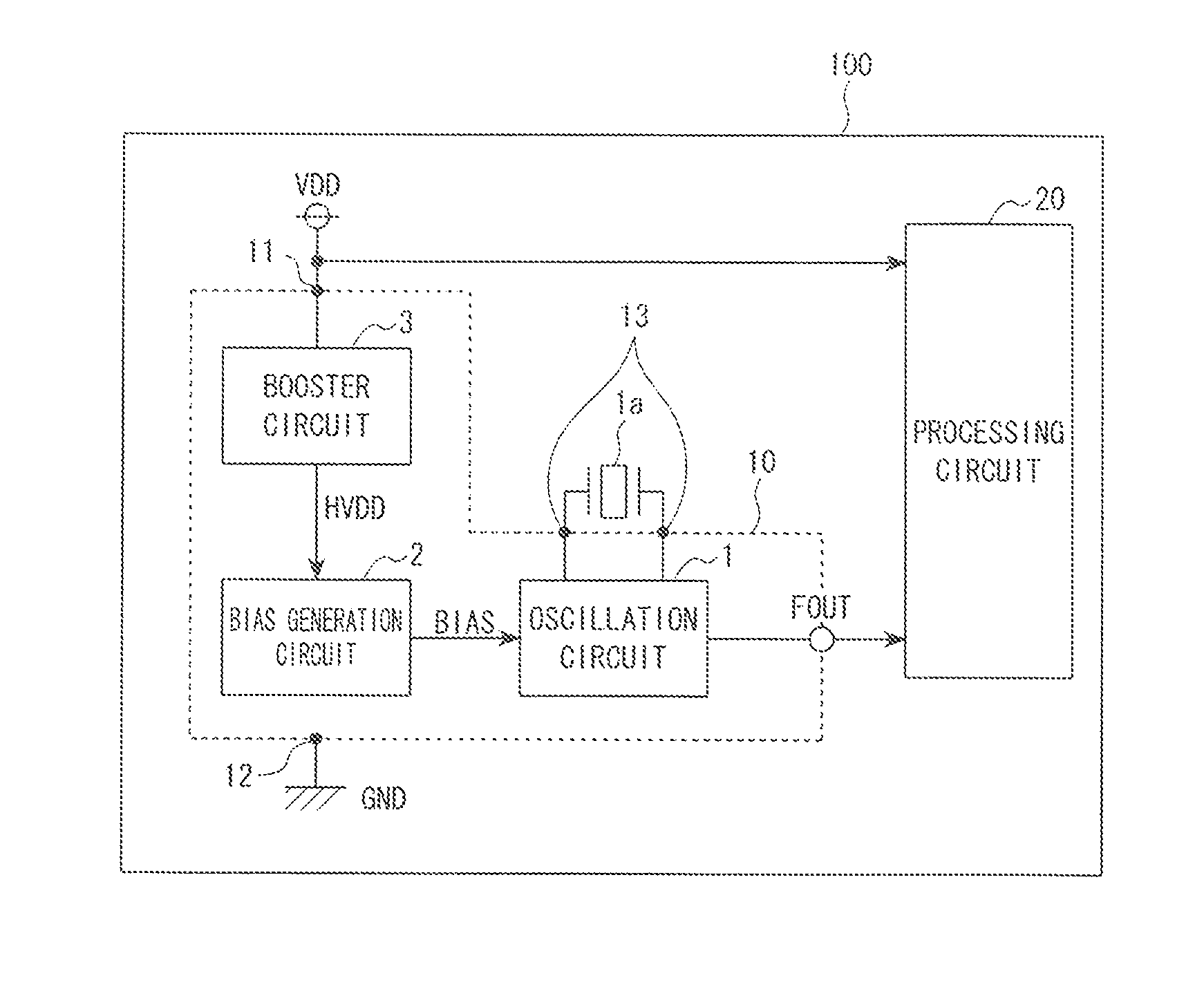
[0039]FIG. 1 is a block diagram illustrative of a configuration example of a crystal oscillator according to a first embodiment of the present invention. FIG. 1 illustrates a case where a crystal oscillator (an oscillator) according to the first embodiment is mounted on an IC chip 10 and located on a mounted substrate 100 in an electronic device. In addition to IC chip 10, an IC chip 20 having a processing circuit mounted thereon is located on the mounted substrate 100. The processing circuit of the IC chip 20 receives an output frequency from the crystal oscillator of the IC chip 10 to perform processing of an input / output device or the like. Further, in FIG. 1, a crystal oscillation unit la is located on the mounted substrate 100 and arranged at the exterior of the IC chip 10. However, the IC chip 10 and the crystal oscillation unit la may be mounted in an identical module.

[0040]The crystal oscillator according to the first embodiment mounted on the IC chip 10 is provided with: an...

second embodiment

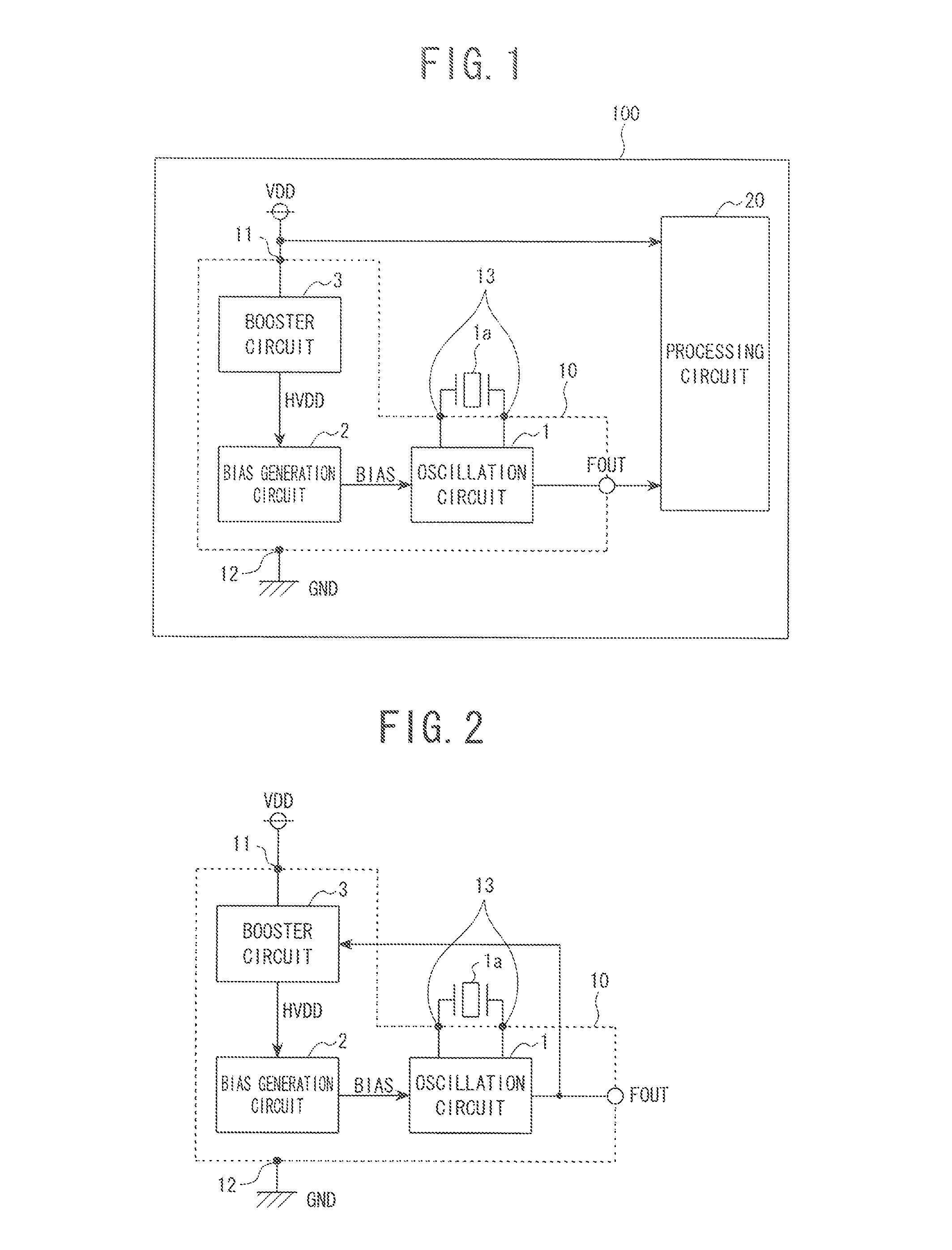
[0049]FIG. 2 is a block diagram illustrative of a configuration example of a crystal oscillator according to a second embodiment of the present invention. In FIG. 2, the configuration other than the IC chip 10 on the mounted substrate 100 is omitted, and only the configuration of the IC chip 10 on which the crystal oscillator is mounted is illustrated (this applies to other embodiments). The crystal oscillator according to the second embodiment illustrated in FIG. 2 has a substantially similar configuration to that of the crystal oscillator according to the first embodiment, but has a different configuration in that the booster circuit 3 is driven by an output signal from the oscillation circuit 1.

[0050]That is, the booster circuit 3 performs a boosting operation with the output signal from the oscillation circuit 1 as a clock. Thus, spurious tones generated at the output voltage (boosted voltage HVDD) from the booster circuit 3 are only integral multiples of the oscillation frequen...

third embodiment

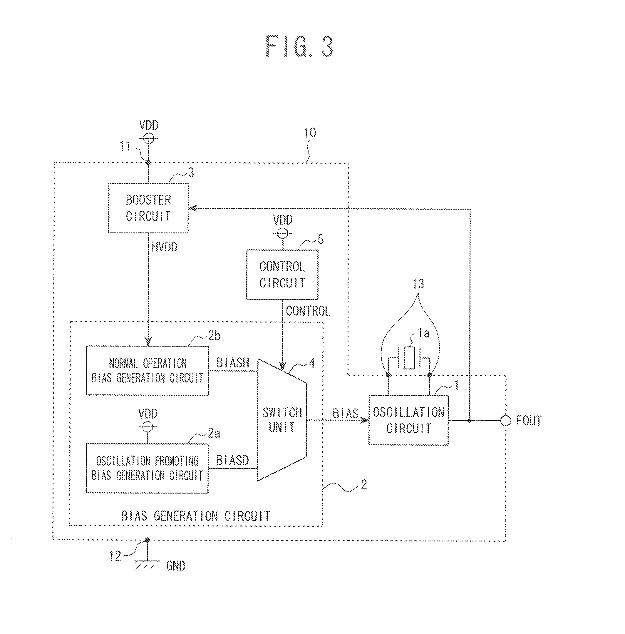
[0052]FIG. 3 is a block diagram illustrative of a configuration example of a crystal oscillator according to a third embodiment of the present invention. Referring to FIG. 3, the bias generation circuit 2 constituting the crystal oscillator according to the third embodiment is provided with: an oscillation promoting bias generation circuit 2a (a first bias circuit); a normal operation bias generation circuit 2b (a second bias circuit); and a switch unit 4. Additionally, the crystal oscillator according to the third embodiment includes a control circuit 5 for controlling the switch unit 4.

[0053]The oscillation promoting bias generation circuit 2a is driven by the power supply voltage VDD to output bias BIASD such that the negative resistance of the crystal oscillator is improved to promote the oscillation. On the other hand, the normal operation bias generation circuit 2b is driven by the boosted voltage HVDD to output bias BIASH such that the crystal oscillator performs a normal ope...


PUM


Abstract

There is provided an oscillator capable of lowering the power supply voltage without degrading the phase noise, while employing the conventional circuit configuration. According to one aspect of the present invention, there is provided an oscillator comprising: an oscillation circuit; a bias generation circuit for generating a bias signal to drive the oscillation circuit; and a booster circuit for boosting a power supply voltage to generate a boosted voltage for driving the bias generation circuit. In addition, the oscillation circuit, the bias generation circuit, and the booster circuit are provided in a single IC chip, and the booster circuit may receive the power supply voltage VDD from the power supply arranged at the exterior of the IC chip.

Description

TECHNICAL FIELD[0001]The present invention relates to oscillators for oscillating frequency signals and IC chips.BACKGROUND ART[0002]Temperature Compensated Crystal Oscillator (TCXO) enables stable output frequencies in response to changed in ambient air temperatures. Therefore, TCXO is widely used for a mobile telephone, a Personal Navigation Device (PND), and the like.[0003]In recent years, higher functions and longer life of operable period are demanded for these devices, whereas their mounted components are required to lower the power consumption. Conventionally, the low power consumption has been promoted by sampling action of TCXO. In order to achieve further lower power consumption, however, operation of TCXO at low voltages is requested. As a conventional oscillator with such a temperature compensated crystal oscillator, there is an example of an oscillator in Patent Document 1.[0004]FIG. 7 is a configuration diagram illustrative of main components of an oscillator described...

Claims


Application Information

Patent Timeline
IPC IPC(8): H03L1/04
CPCH03L1/04H03B5/04H03B5/36H03B2200/0082
Inventor MARU, HARUHIKO
Owner ASAHI KASEI ELECTRONICS CO LTD
Why Eureka
Try Eureka