Liquid crystal display device and method for repairing the same

a technology of liquid crystal display and lcd, which is applied in the direction of optics, instruments, electrical equipment, etc., can solve the problems of lcd device, hot pixel or dead pixel, switching device not being normally driven, etc., and achieve the effect of enhancing the repair ra

Active Publication Date: 2013-08-22
LG DISPLAY CO LTD
View PDF2 Cites 28 Cited by
  • Summary
  • Abstract
  • Description
  • Claims
  • Application Information

AI Technical Summary

Benefits of technology

[0019]Accordingly, one aspect of the present invention is to provide a liquid crystal display (LCD) device capable of enhancing a repair rate by electrically contacting a pixel electrode and a common electrode with each other through a floating electrode.

Problems solved by technology

However, the LCD device has the following problems.
Further, a thin film transistor (TFT) may not be normally driven due to conductive foreign materials remaining at an LC panel, resulting in a hot pixel or a dead pixel.
However, in the rework process, the switching device may not be normally driven due to foreign materials remaining thereon.
Furthermore, if the first and second substrates are attached to each other when foreign materials remain on the switching device, a rework process cannot be performed.
Furthermore, the repair process has a difficulty in passing through a thick film including a passivation layer and a gate insulating film each disposed between the pixel electrode 15 and the common electrode 60.
It is also difficult to perform a welding process with respect to the pixel electrode 15 and the common electrode 60 each formed of a thin film having a thickness of 300 Ř400 Å.

Method used


Image

  • Liquid crystal display device and method for repairing the same
  • Liquid crystal display device and method for repairing the same
  • Liquid crystal display device and method for repairing the same

Examples


first embodiment

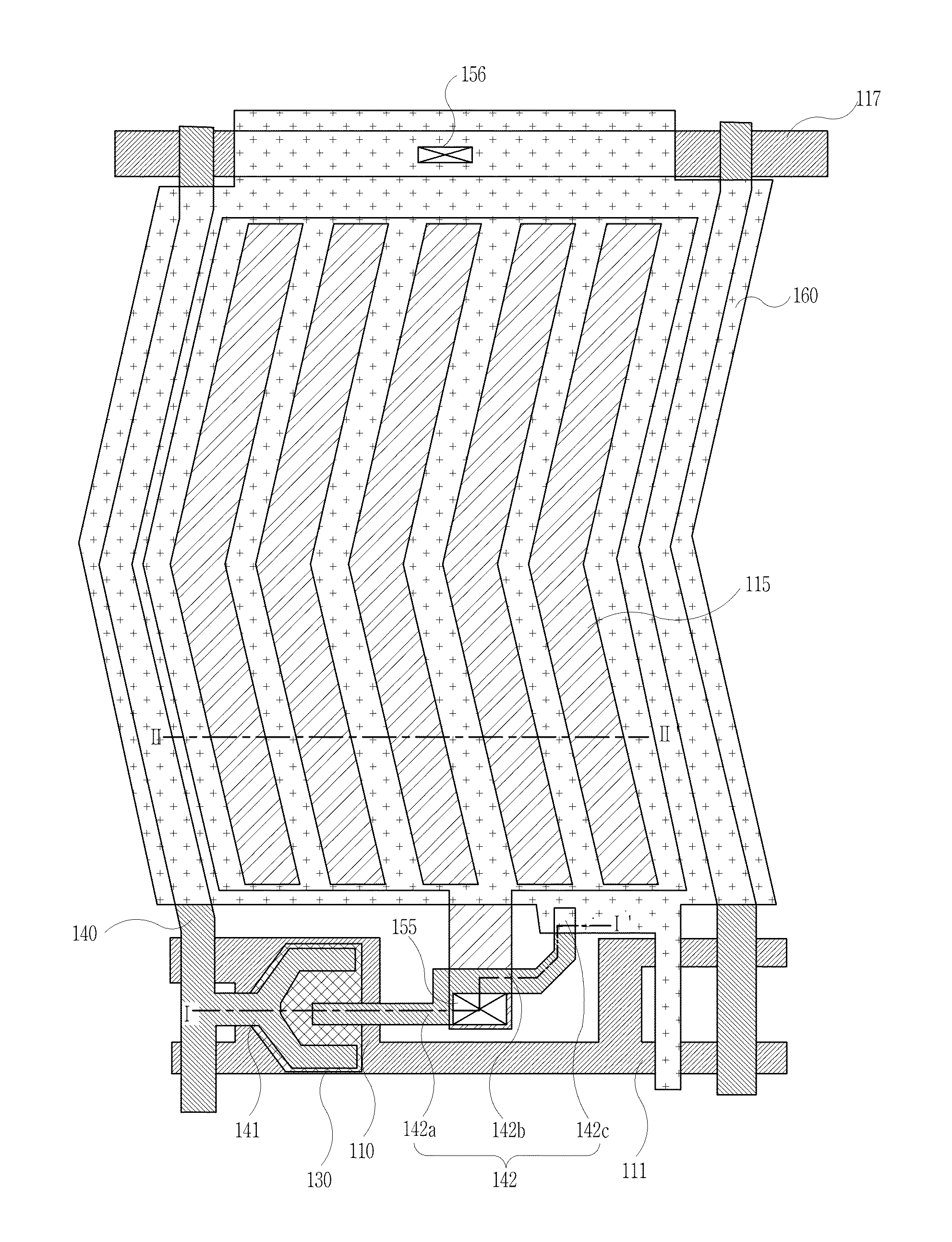
[0045]Referring to FIG. 4B, the active layer 130 is preferably formed to entirely overlap the drain electrode 142. This results from the drain electrode 142 and the active layer 130 being formed using the same mask. However, the present invention is not limited to this. That is, the active layer 130 may be formed to partially overlap the drain electrode 142.

[0046]Referring to FIG. 4A, the pixel electrode 115 is formed in a single pattern so as to correspond to a transmissive region of a unit pixel. Referring to FIG. 4B, the pixel electrode 115 is formed at the same layer as the gate electrode 110 on the first substrate 100. The pixel electrode 115 is also electrically connected to the drain electrode 142 via a connection pattern 161 of the first contact hole 155, and receives a data voltage from the drain electrode 142.

[0047]Further, the first contact hole 155 is formed through the first insulating layer 120, the active layer 130, the drain electrode 142 and a second insulating laye...

second embodiment

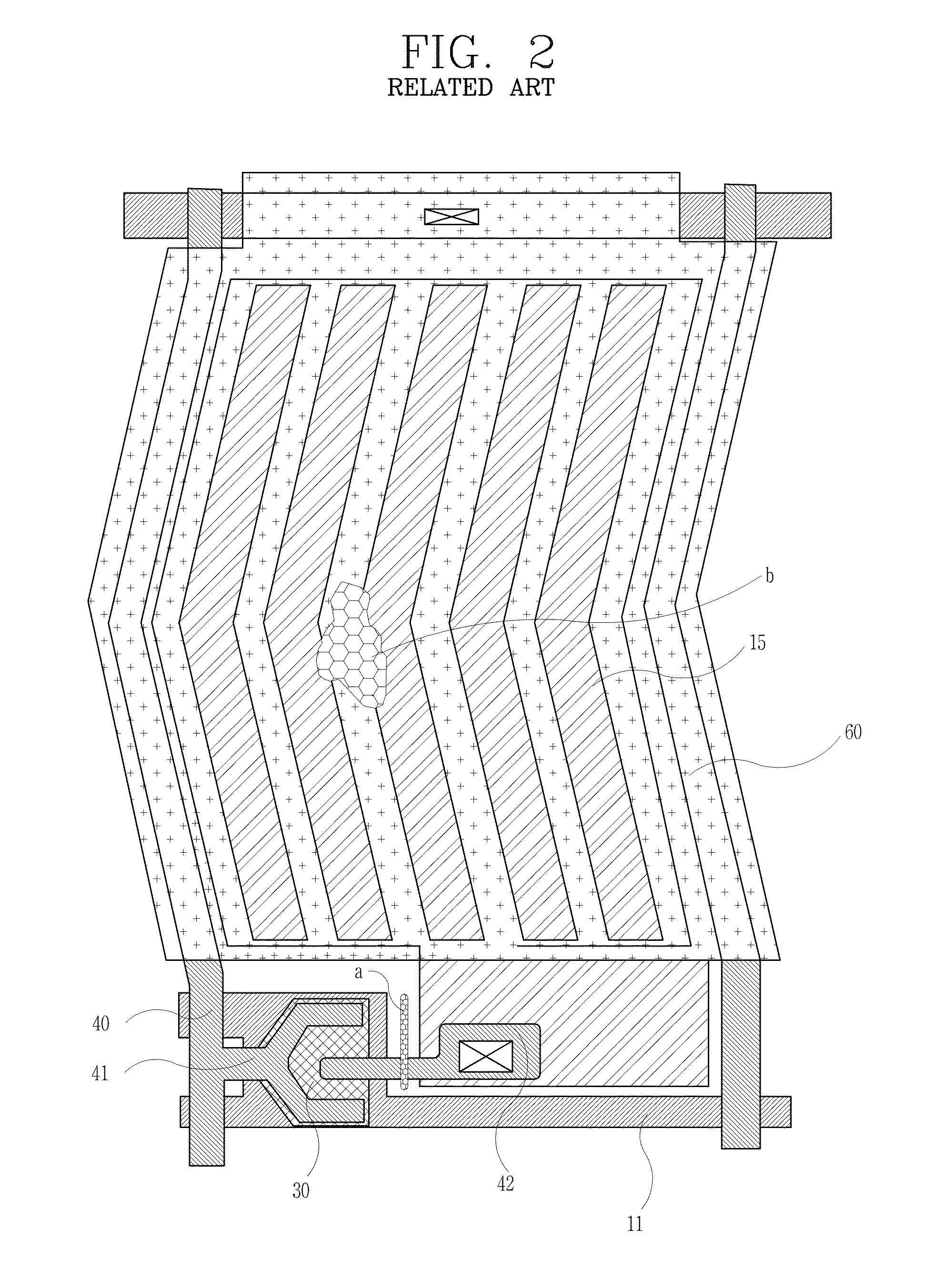
[0072]An active layer 230, contact hole 255 and connection pattern 261 are also shown in this In addition, the cutting region is a region ‘A2’, which is a region where the first drain electrode portion 242a has been formed. The region ‘A2’ may also be a region not overlapping a gate electrode 210, among regions where the first drain electrode portion 242a has been formed.

[0073]Then, the gate line 211 is cut at regions ‘B2’ and ‘C2’, thereby being in a floating state. Referring to FIG. 7A, the floating gate line 211 indicates part of the gate line 211 formed at an overlapping region between the third drain electrode portion 242c and the common electrode connection line 260a. Referring to FIG. 7B, the first insulating layer 220 is disposed between the floating gate line 211 and the third drain electrode portion 242c. In addition, the first insulating layer 220 and the second insulating layer 250 are disposed between the floating gate line 211 and the common electrode connection line ...


PUM

PropertyMeasurementUnit
widthaaaaaaaaaa
vertical widthaaaaaaaaaa
widthaaaaaaaaaa

Abstract

A liquid crystal display device including a cut portion at a position not overlapping the gate electrode such the pixel electrode is floating and does not receive a voltage from the source electrode via the active layer and the drain electrode; a second insulating layer above the first insulating layer; a plurality of common electrodes on the second insulating layer; and a welded portion at a region where a corresponding common electrode overlaps the drain electrode. Further, the drain electrode and the pixel electrode are electrically connected to each other via a connection pattern formed in a contact hole such that the welded portion floats the pixel electrode.

Description

CROSS-REFERENCE TO A RELATED APPLICATION[0001]Pursuant to 35 U.S.C. §119(a), this application claims the benefit of earlier filing date and right of priority to Korean Application No. 10-2012-0018189, filed on Feb. 22, 2012, the contents of which is incorporated by reference herein in its entirety.BACKGROUND OF THE INVENTION[0002]1. Field of the Invention[0003]The present invention relates to a liquid crystal display (LCD) device and a method for repairing the same, and more particularly, to an LCD device in which a hot pixel is repaired into a dead pixel, and a method for repairing the same.[0004]2. Background of the Invention[0005]Flat display devices including a Liquid Crystal Display (LCD) device, a Plasma Display Panel (PDP), an Electro Luminescent Display (ELD), a Vacuum Fluorescent Display (VFD), etc. have been proposed. Among such flat display devices, the LCD device is being most widely used due to its advantages such as an excellent picture quality, a light weight, a thin ...

Claims


Application Information

Patent Timeline
Patent Type & Authority Applications(United States)
IPC IPC(8): G02F1/13G02F1/1362G02F1/1368
CPCG02F1/1309G02F1/1368Y10T29/49002G02F1/136227G02F1/136259G02F1/136286G02F1/13G02F1/1343
Inventor YOON, HYUNMYOUNGCHOI, ILMANKANG, MOONSOOCHO, HWIJE
Owner LG DISPLAY CO LTD
Why Eureka
Try Eureka