
Copper foil for printed wiring board, method for producing said copper foil, resin substrate for printed wiring board and printed wiring board
a technology of printed wiring and resin substrate, which is applied in the direction of cable/conductor manufacturing, metallic pattern materials, and record information storage, etc., can solve the problems of increasing the number of steps, not being suitable for a stable circuitry design, and not being able to detect the impedance. , to achieve the effect of higher frequency
- Summary
- Abstract
- Description
- Claims
- Application Information
AI Technical Summary
Benefits of technology
Problems solved by technology
Method used
Image

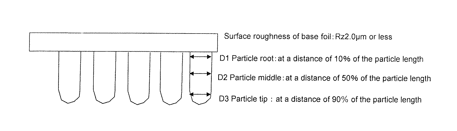
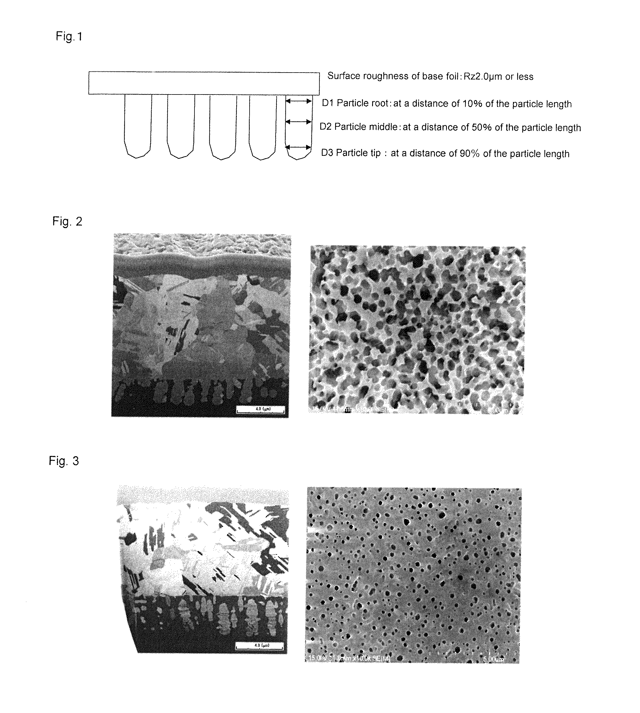
Examples
example 1
[0096]Using a 12 μm-thick electrolytic copper foil (the roughness of a surface on which a roughened copper layer is formed: Rz 0.6 μm), roughening plating was performed on the rough surface (namely ‘matte surface’ or ‘M surface’) of this copper foil as described below. The treatment conditions are shown below. Each of these is a step for forming a roughened layer on the copper foil of the present invention. The ratio to the limiting current density when forming roughening particles was 2.50.
[0097]CuSO4.5H2O: 58.9 g / L
[0098]Cu: 15 g / L
[0099]H2SO4: 100 g / L
[0100]Na2WO4.2H2O: 5.4 mg / L
[0101]W: 3 mg / L
[0102]Added amount of sodium dodecyl sulfate: 10 ppm
[0103](Electroplating Temperature 1) 50° C.
[0104]Normal plating as shown below was performed after the present roughening treatment. The treatment conditions are shown below.
[0105]CuSO4′5H2O: 156 g / L
[0106]Cu: 40 g / L
[0107]H2SO4: 100 g / L
[0108](Electroplating Temperature 1) 40° C.
(Electric Current Condi...
example 2
[0128]Using a 12-μm thick electrolytic copper foil, roughening plating as described below and normal plating as in Example 1 were performed on a rough surface (a matte surface) of that copper foil. The treatment conditions for roughening plating are shown below. Each of these is a step for forming a roughened layer on the copper foil of the present invention. The ratio to the limiting current density when forming roughening particles was 3.10.
[0129]CuSO4.5H2O: 58.9 g / L
[0130]Cu: 15 g / L
[0131]H2SO4: 100 g / L
[0132]Na2WO4.2H2O: 5.4 mg / L
[0133]W: 3 mg / L
[0134]Added amount of sodium dodecyl sulfate: 10 ppm
[0135](Electroplating Temperature 1) 50° C.
[0136]The surface roughness Rz of this roughened layer is 1.51 μm, and the average diameter at the particle root (D1) is 0.51 μm, and the particle length (L1) is 2.68 μm, and the ratio to the average diameter at the particle root (D1) is 5.21 when L1 / D1. Needle-like or rod-like particles appear to be formed by the look of FIG. ...
example 3
[0142]Using a 12-μm thick electrolytic copper foil, roughening plating as described below and normal plating as in Example 1 were performed on a rough surface (a matte surface) of that copper foil. The treatment conditions for roughening plating are shown below. Each of these is a step for forming a roughened layer on the copper foil of the present invention. The ratio to the limiting current density when forming roughening particles was 4.30.
(Liquid Composition 1)
[0143]CuSO4.5H2O: 58.9 g / L
[0144]Cu: 15 g / L
[0145]H2SO4: 100 g / L
[0146]Na2WO4.2H2O: 5.4 mg / L
[0147]W: 3 mg / L
[0148]Added amount of sodium dodecyl sulfate: 10 ppm
[0149](Electroplating Temperature 1) 50° C.
[0150]The surface roughness Rz of this roughened layer is 1.56 μm, and the average diameter at the particle root (D1) corresponding to a distance of 10% of a particle length is 0.59 μm. The particle length (L1) is 2.68 μm, and the ratio to the average diameter at the particle root (D1) is 4.52 when L1 / D1. By the look of FIG. 2,...
PUM
| Property | Measurement | Unit |
|---|---|---|
| Length | aaaaa | aaaaa |
| Length | aaaaa | aaaaa |
| Fraction | aaaaa | aaaaa |
Abstract
Description
Claims
Application Information