Display device, and process for manufacturing display device

Inactive Publication Date: 2013-08-29
SHARP KK
View PDF4 Cites 26 Cited by
  • Summary
  • Abstract
  • Description
  • Claims
  • Application Information

AI Technical Summary

Benefits of technology

[0032]The display device of the present invention includes: a plurality of input detection electrodes, which are provided in a display area, for detecting an input on a display surface; a display panel; and a plurality of optical plate members that are stacked on the display panel and contribute to a display or to improvement in display quality, at least one of the plurality of input detection electrodes being provided on at least one of the plurality of optical plate members.
[0033]The method of the present invention for manufacturing a display device is a method for manufacturing a display devi

Problems solved by technology

This causes problems of deteriorati

Method used


Image

  • Display device, and process for manufacturing display device
  • Display device, and process for manufacturing display device
  • Display device, and process for manufacturing display device

Examples


embodiment 1

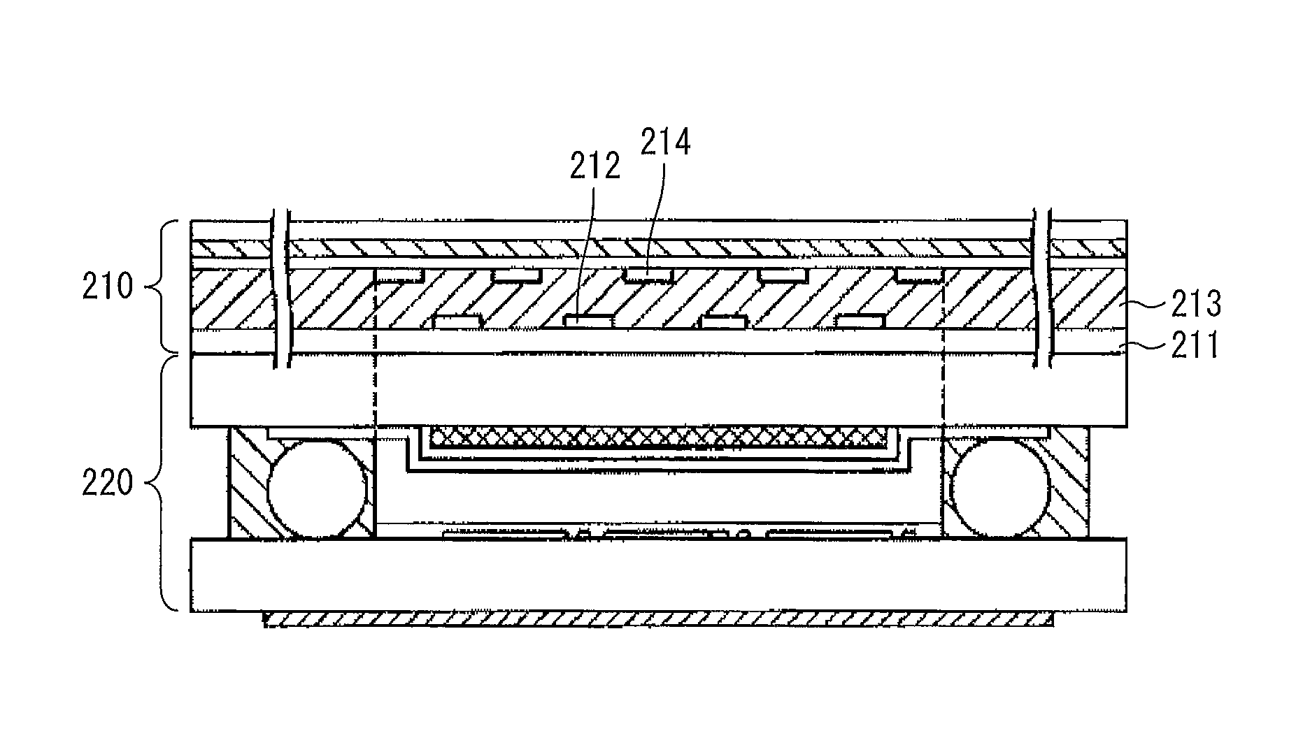
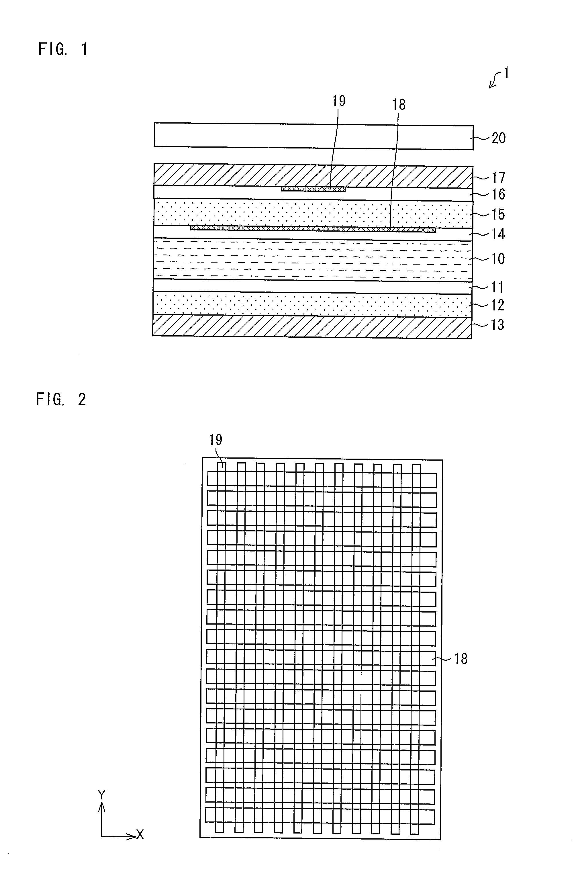
[0055]The following description will discuss a display device in accordance with an embodiment of the present invention, with reference to FIGS. 1, 2, and 9. Note that, in Embodiment 1, an example is described in which a liquid crystal display device is employed as the display device.

[0056]FIG. 1 is a cross sectional view illustrating a configuration of the liquid crystal display device in accordance with Embodiment 1.

[0057]In a liquid crystal display device 1, a touch panel and a display device are integrated (see FIG. 1), unlike a conventional configuration in which a touch panel is stacked on a display device.

[0058]Specifically, the liquid crystal display device 1 includes a liquid crystal panel 10 which is made up of a TFT substrate (not illustrated in FIG. 1) and a counter substrate (not illustrated in FIG. 1) which are joined together by a sealant, and a liquid crystal layer (not illustrated in FIG. 1) is sealed in a space demarcated by the sealant.

[0059]The following descript...

modified example 1

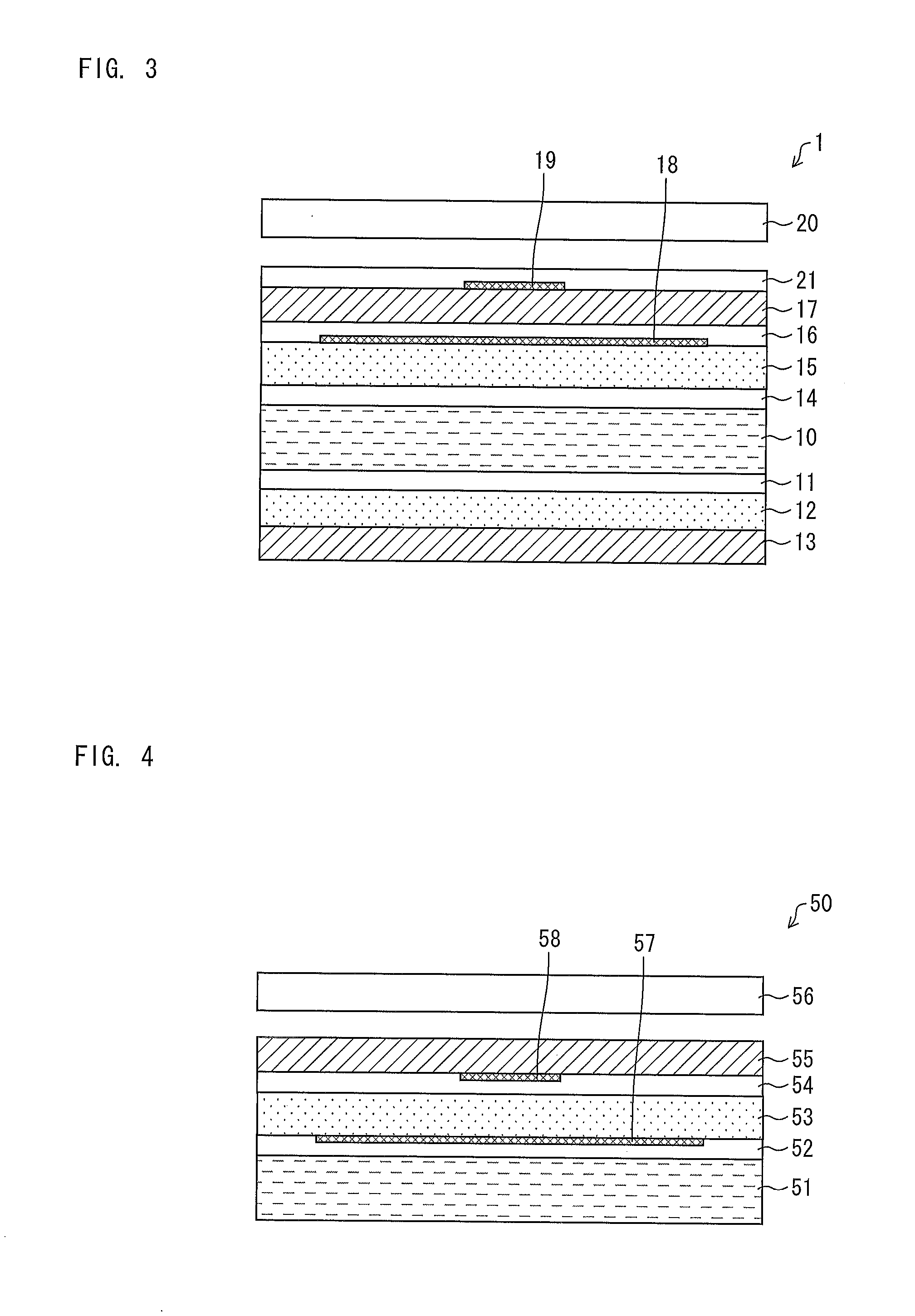
[0087]The following description will discuss a modified example of the liquid crystal display device of Embodiment 1, with reference to FIG. 3. FIG. 3 is a cross sectional view illustrating a configuration of a liquid crystal display device in accordance with Modified Example 1.

[0088]Note that, for convenience, the same reference numerals are given to constituent members which have functions identical with those of constituent members described in Embodiment 1.

[0089]In Modified Example 1, locations of the X electrode 18 and the Y electrode 19 are different from those in Embodiment 1.

[0090]Specifically, in Modified Example 1, the X electrode 18 is provided on a surface of the phase plate 15 which surface faces the polarizing plate 17, and the Y electrode 19 is provided on a surface of the polarizing plate 17 which surface faces the cover glass 20, unlike Embodiment 1 in which the X electrode 18 is provided on a surface of the phase plate 15 which surface faces the liquid crystal pane...

embodiment 2

[0098]The following description will discuss a display device in accordance with another embodiment of the present invention, with reference to FIGS. 4, 5, and 10. In Embodiment 2, an example is described in which an organic EL display device is employed as the display device. In the organic EL display device, a circularly polarizing plate made up of a polarizing plate and a λ / 4 plate (quarter wave plate) is attached to an upper surface of an organic EL panel for preventing reflection light.

[0099]FIG. 10 is a cross sectional view illustrating a configuration of an organic EL panel 51. The organic EL panel 51 includes a glass substrate 51a, TFTs 51b, organic EL layers 51c, an adhesion layer 51d, and a sealing substrate 51e. The TFTs 51b are provided for respective pixels and serve as switching elements. The organic EL layers 51c are provided for the respective pixels. The adhesion layer 51d is provided so as to cover the organic EL layers 51c. The sealing substrate 51e is made up of ...


PUM

PropertyMeasurementUnit
Thicknessaaaaaaaaaa

Abstract

An X electrode (18) is provided on a surface of a phase plate (15) which surface faces a liquid crystal panel (10). A Y electrode (19) is provided on a surface of a polarizing plate (17) which surface faces the liquid crystal panel (10). This makes it possible to provide a display device that has a touch function and can reduce a thickness and improve display quality.

Description

TECHNICAL FIELD [0001]The present invention relates to a display device and a method for manufacturing a display device. In particular, the present invention relates to a display device having a touch function and a method for manufacturing such a display device.BACKGROUND ART [0002]In display devices, touch panels are often provided so that a user can easily operate the display device while viewing its screen.[0003]There have already been various types of touch panels in practical use. In recent years, capacitive touch panels are becoming popular. According to a capacitive touch panel, when a fingertip (which can be considered as an electric conductor) makes contact with a touch input surface, a capacitor is formed by a capacitive coupling of the fingertip and a conductive film. In the capacitive touch panel having such a configuration, coordinates of a contact location of the fingertip are detected by sensing a change in electric charge at the contact location.[0004]In particular,...

Claims


Application Information

Patent Timeline
IPC IPC(8): G06F3/041
CPCG02F1/13338G02F1/134336Y10T29/49155G06F3/044H01L27/323G06F3/0412G06F3/0445G06F3/0446H10K59/40
Inventor ABIRU, MANABUKIDA, KAZUTOSHIYAMAGISHI, SHINJI
Owner SHARP KK
Why Eureka
Try Eureka