Memory Diodes

a memory diode and diode technology, applied in the field of memory diodes, can solve the problems of microelectronics industry, memory industry problems, and memory industry scaling limitations,

Inactive Publication Date: 2013-09-12
TECHNION RES & DEV FOUND LTD
View PDF4 Cites 5 Cited by
  • Summary
  • Abstract
  • Description
  • Claims
  • Application Information

AI Technical Summary

Benefits of technology

[0057]connecting a second non-insulator, different from the first non-insulator, to form a junction with the first non-insulator, at least one of the first and second non-insulators b

Problems solved by technology

However, known technological and scaling limitations of the memories based on existing technologies, such as flash

Method used


Image

  • Memory Diodes
  • Memory Diodes
  • Memory Diodes

Examples


examples

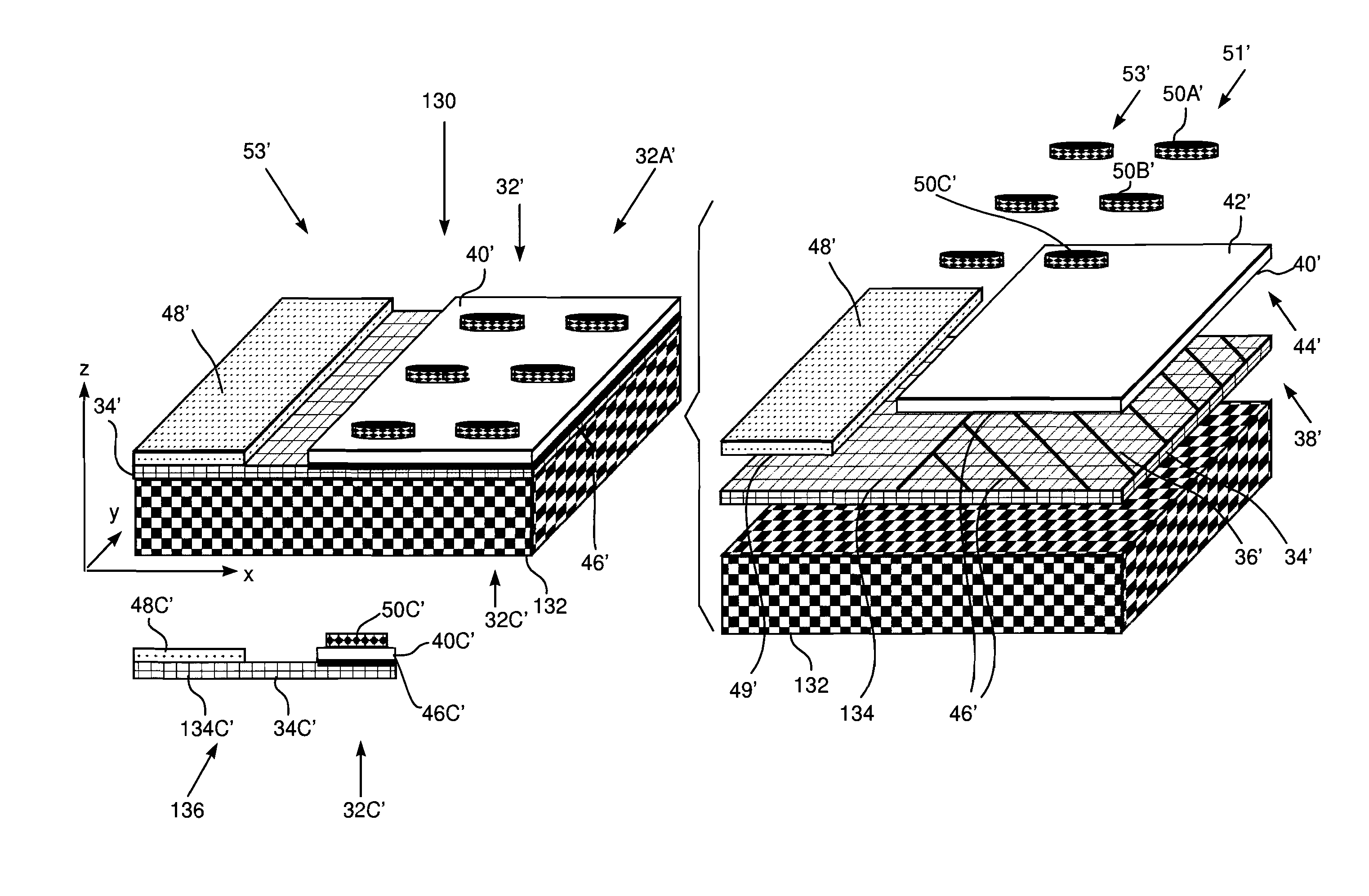
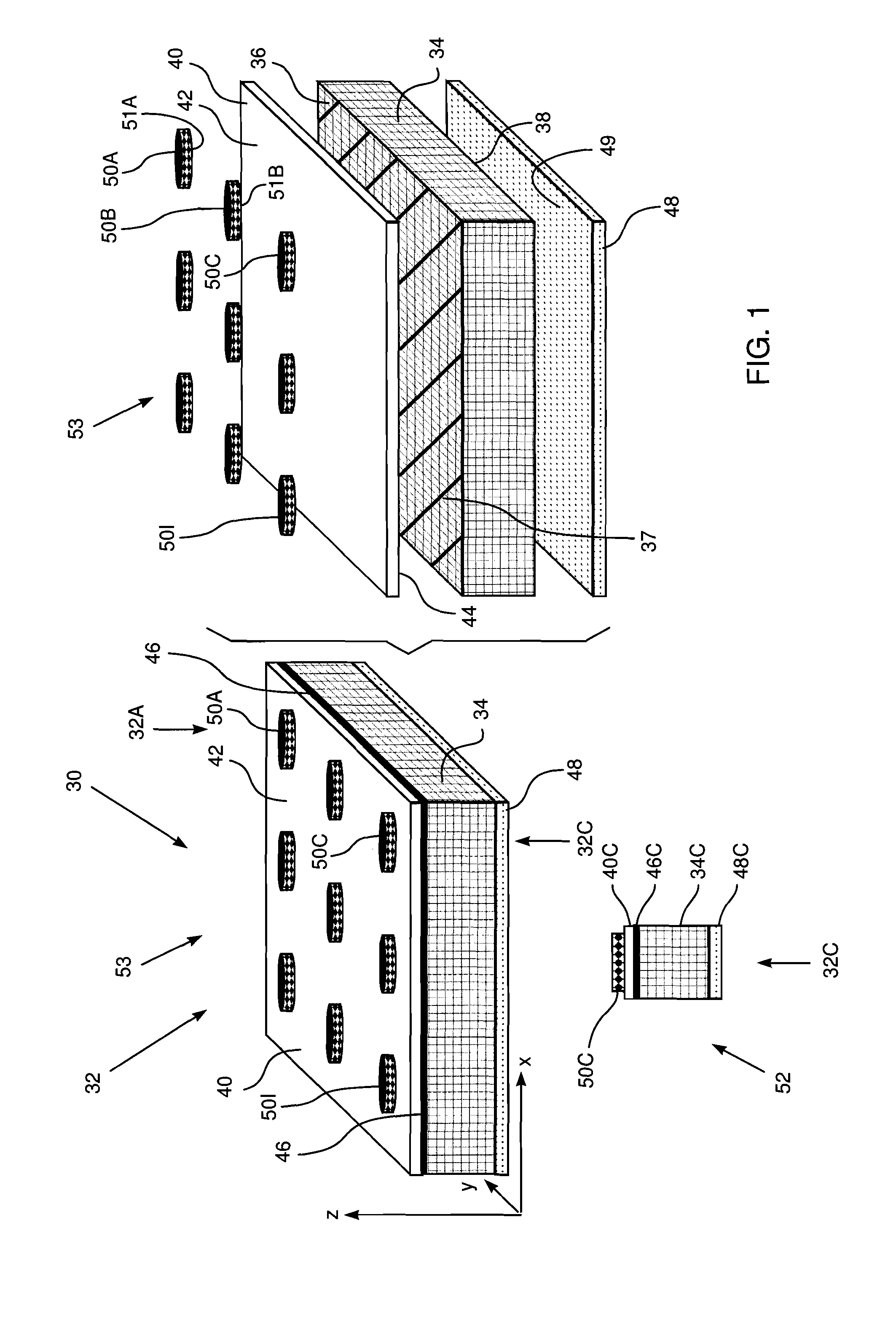
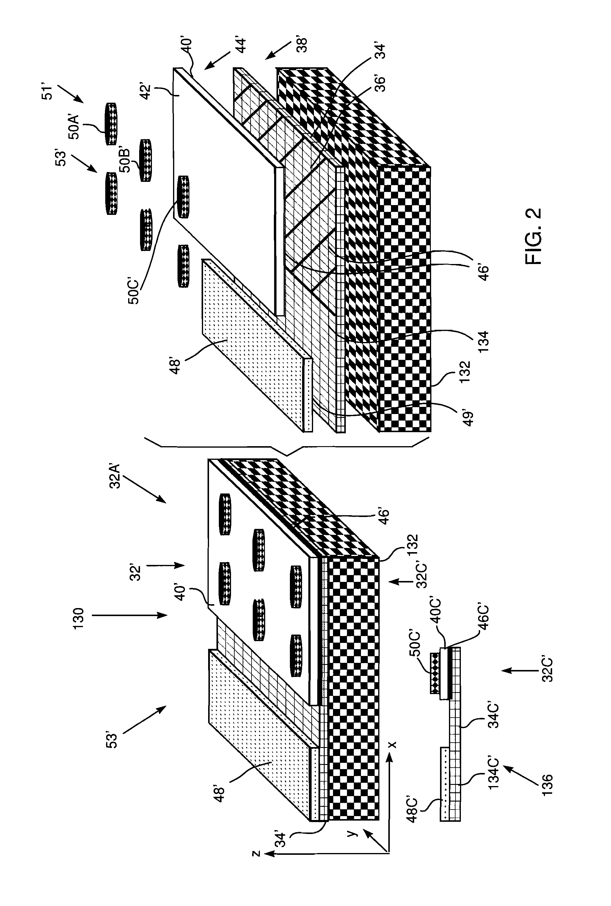
[0128]Single cells having p-n junctions were prepared as follows. A first cell corresponded to a cell of single film array 30, a second cell corresponded to a cell of dual film array 130 (FIG. 1 and FIG. 2).

[0129]SrTiO3 thin layers (˜80 nm or ˜160 nm thick), doped with Fe or Nb, were deposited on polished 1.4% Nb-doped (single film configuration, FIG. 1) and undoped (dual film configuration, FIG. 2) SrTiO3 (100) single crystals, 1×1 cm2 in area and 0.5 mm thick, purchased from Crystal Gmbh, of Berlin, Germany. The layers were deposited by pulsed laser deposition (PLD) using commercial 0.1% Fe or Nb-doped SrTiO3 ceramic targets purchased from SCI Engineering Inc. of St. Charles, Mo. The layers were grown in oxygen at a pressure of 55 mTorr (single film configuration) or in high vacuum at ˜10−6 Torr (dual film configuration), and at a substrate temperature of 700° C.

[0130]6000 or 3000 pulses of a KrF excimer laser (λ=248 nm) with an energy flux of 1 J / cm2 and a repetition rate of 3 Hz...


PUM


Abstract

A memory cell (32C), including a first non-insulator (34C) and a second non-insulator (40C), different from the first non-insulator. The second non-insulator forms a junction (46C) with the first non-insulator. The cell further includes a first electrode (48C) which is connected to the first non-insulator and a second electrode (50C) which is connected to the second non-insulator. At least one of the first and second non-insulators is chosen from a group consisting of a solid electrolyte and a mixed ionic electronic conductor and has an ionic transference number less than 1 and greater than or equal to 0.5.

Description

CROSS-REFERENCE TO RELATED APPLICATION[0001]This application claims the benefit of U.S. Provisional Patent Application 61 / 384,589, filed 20 Sep. 2010, which is incorporated herein by referenceFIELD OF THE INVENTION[0002]The present invention relates generally to memory devices, and particularly to memory devices formed from non-insulating materials.BACKGROUND OF THE INVENTION[0003]A number of different memory systems are known in the art. However, known technological and scaling limitations of the memories based on existing technologies, such as flash memories, generate problems for the microelectronics industry. The problems are compounded for the memory industries.[0004]Documents incorporated by reference in the present patent application are to be considered an integral part of the application except that to the extent any terms are defined in these incorporated documents in a manner that conflicts with the definitions made explicitly or implicitly in the present specification, o...

Claims


Application Information

Patent Timeline
IPC IPC(8): H01L45/00
CPCG11C13/00H01L45/1253G11C13/0004G11C13/0002G11C11/36G11C13/0007H10N70/245H10N70/841
Inventor ROTHSCHILD, AVNER
Owner TECHNION RES & DEV FOUND LTD
Why Eureka
Try Eureka