Vertical trench IGBT and method for manufacturing the same

a technology of vertical trenches and bipolar transistors, which is applied in the direction of basic electric elements, electrical equipment, and semiconductor devices, can solve the problems of increased leak current, increased si substrate defects, and inability to shallowly form the emitter layer, and achieve the effect of improving the rbsoa capacity

Active Publication Date: 2013-09-12
MITSUBISHI ELECTRIC CORP
View PDF4 Cites 6 Cited by
  • Summary
  • Abstract
  • Description
  • Claims
  • Application Information

AI Technical Summary

Benefits of technology

[0010]The present invention makes it p

Problems solved by technology

The emitter layer cannot be shallowly formed because of impurity injection and heat treatment.
In addition, when stress is concentrated in the bottom of t

Method used


Image

  • Vertical trench IGBT and method for manufacturing the same
  • Vertical trench IGBT and method for manufacturing the same
  • Vertical trench IGBT and method for manufacturing the same

Examples


first embodiment

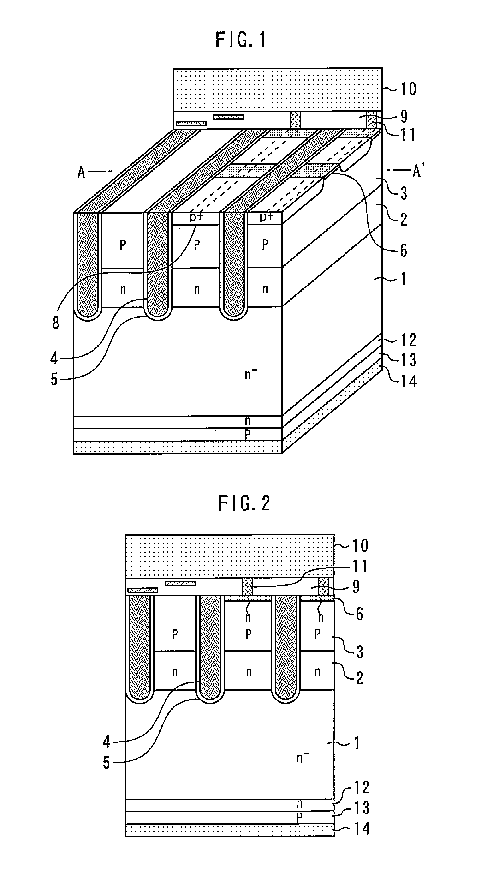
[0022]FIG. 1 is a perspective view showing a vertical trench IGBT according to the first embodiment of the present invention. FIG. 2 is a sectional view taken along the line A-A′ in FIG. 1. An n-type charge accumulating layer 2 and a p-type body layer 3 are sequentially provided on the n−-type Si substrate 1. Trench gates 4 are provided in trenches passing through the p-type body layer 3 via gate insulating films 5. The trench gates 4 are provided in stripes in planar view.

[0023]An n-type emitter layer 6 and a p+-type diffusion layer 8 are provided on a p-type body layer 3. In planar view, the n-type emitter layer 6 and the p+-type diffusion layer 8 are alternately arranged between adjacent trench gates 4 in the length direction of the trench gates 4.

[0024]The trench gates 4 are coated by an interlayer insulating film 9. An emitter electrode 10 is provided on the interlayer insulating film 9. Contact plugs 11 pass through the interlayer insulating film 9 and connect the p-type body ...

second embodiment

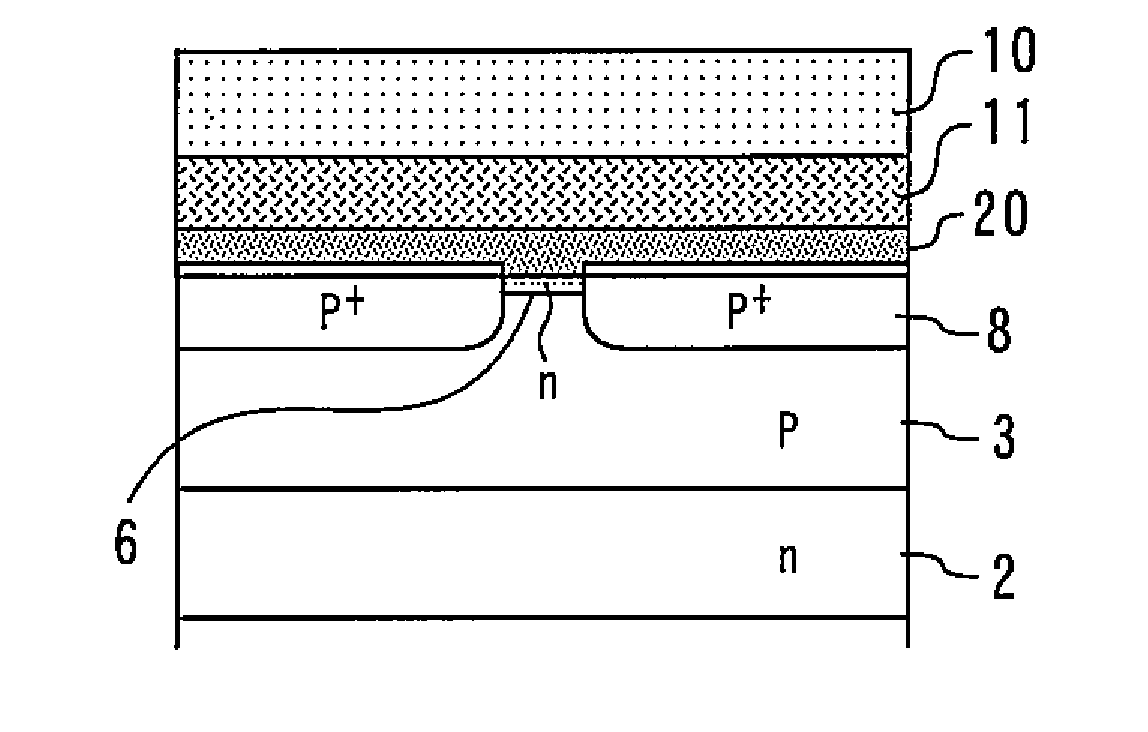
[0035]FIG. 14 is a perspective view showing the vertical trench IGBT according to the second embodiment of the present invention. FIG. 15 is a sectional view taken along the line A-A′ in FIG. 14. A polysilicon film 20 having a film thickness of 500 to 5000 Å is provided between the p-type body layer 3 and between the n-type emitter layer 6 and a contact plug 11.

[0036]By this polysilicon film 20, the stress by the trench gate 4 and the contact plug 11 in fine cells can be reduced. Thereby, increase of the default into the Si substrate can be suppressed. As a result, since the leakage current into connection is reduced, the RBSOA capacity can be improved.

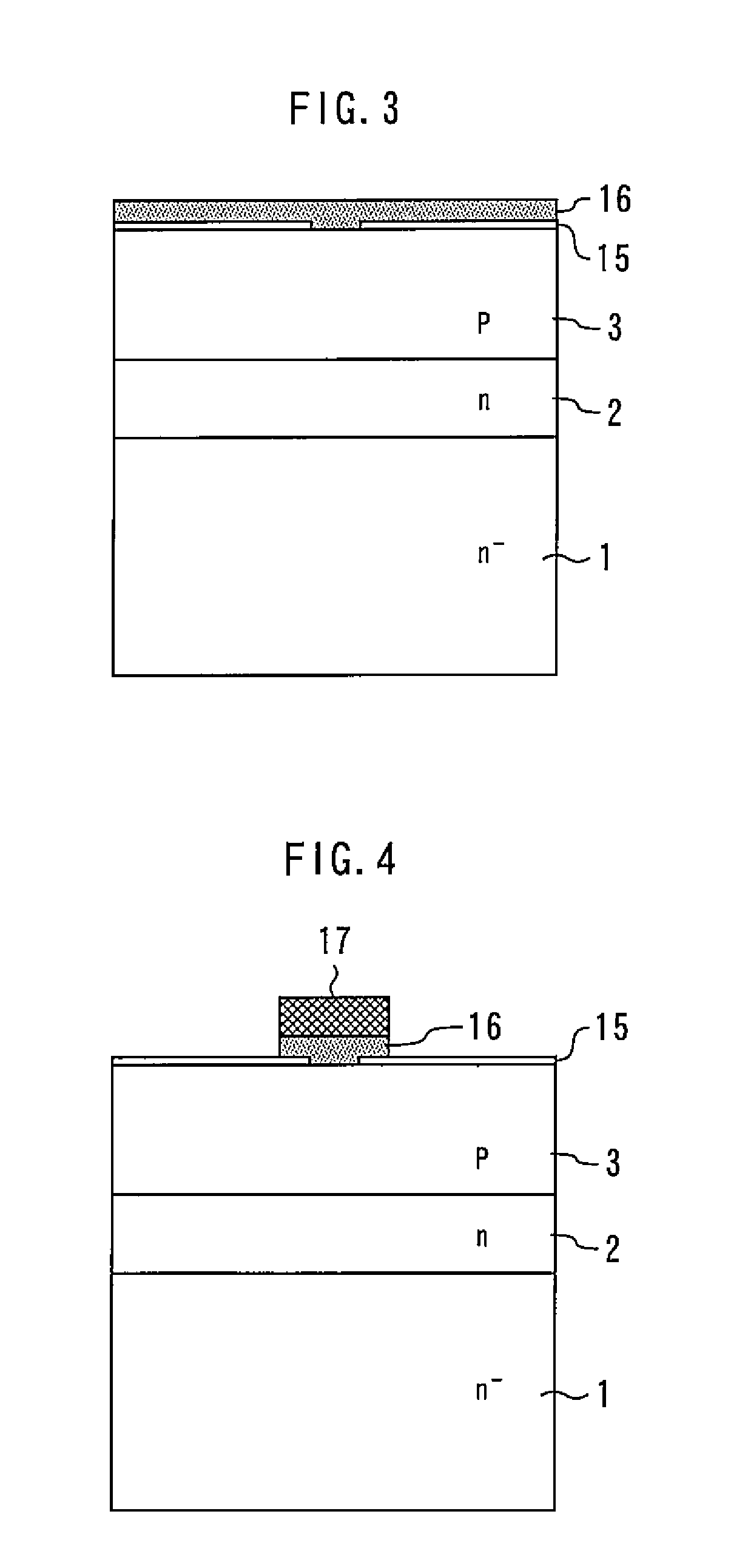
[0037]In addition, in the first and second embodiments, it is favorable that the polysilicon films 16 and 20 are simultaneously formed together with the polysilicon to constitute the trench gate 4, the polysilicon to constitute the electrode 21 of the Poly-Poly capacitor, and a polysilicon resistor 22. Thereby, the number of processes...


PUM


Abstract

A method for manufacturing a vertical trench IGBT includes: forming a body layer of a second conductivity type on a semiconductor substrate of a first conductivity type; forming a trench passing through the body layer; forming a trench gate in the trench via a gate insulating film; forming a polysilicon film containing an impurity of a first conductivity type on the body layer; diffusing the impurity from the polysilicon film into the body layer to form an emitter layer of a first conductivity type on the body layer; and forming a collector layer of a second conductivity type on a lower surface of the semiconductor substrate.

Description

BACKGROUND OF THE INVENTION[0001]1. Field of the Invention[0002]The present invention relates to a vertical trench IGBT (Insulated Gate Bipolar Transistor) and a method for manufacturing the same.[0003]2. Background Art[0004]Conventionally, the emitter layer of a vertical trench IGBT has been formed by impurity injection and heat treatment. For miniaturizing the cell structure of a vertical trench IGBT, the contact structure must use plugs. However, a contact plug has contacted with the semiconductor layer via a thin barrier metal.[0005]In horizontal transistors, the formation of a diffusion layer by impurity diffusion from polysilicon, or the provision of a polysilicon film between a semiconductor layer and a contact plug has been proposed (for example, refer to Japanese Patent Application Laid-Open No. 8-97226, Japanese Patent Application Laid-Open No. 9-246493, and Japanese Patent Application Laid-Open No. 9-92628).SUMMARY OF THE INVENTION[0006]RBSOA (Reverse Biased Safe Operatin...

Claims


Application Information

Patent Timeline
IPC IPC(8): H01L29/739H01L21/331
CPCH01L29/66348H01L29/0839H01L29/0696H01L29/7397H01L21/18H01L29/739
Inventor FUJII, HIDENORI
Owner MITSUBISHI ELECTRIC CORP
Why Eureka
Try Eureka